TDA7496L Просмотр технического описания (PDF) - STMicroelectronics
Номер в каталоге
Компоненты Описание
производитель
TDA7496L Datasheet PDF : 10 Pages
| |||
TDA7496L
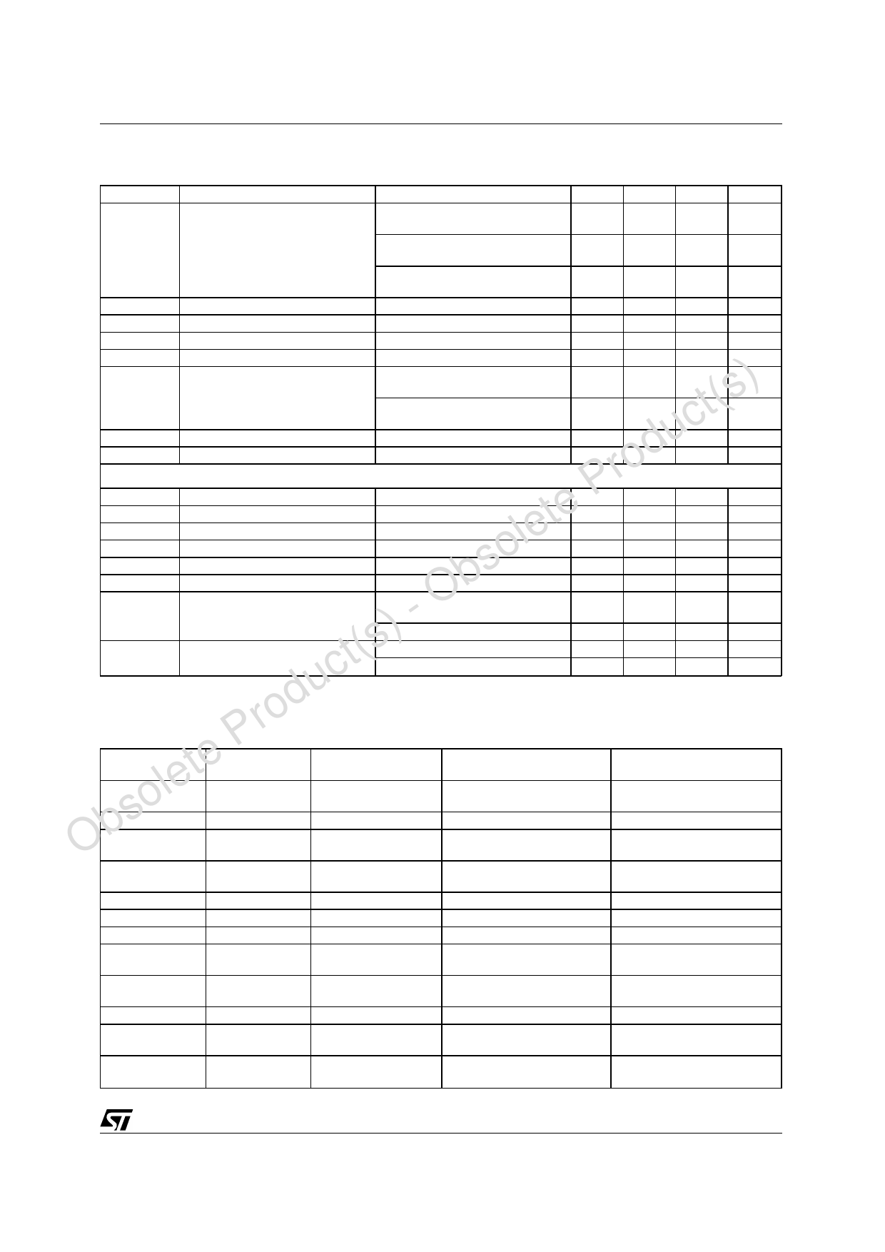
ELECTRICAL CHARACTERISTICS (continued)
Symbol
Parameter
Test Condition
Min. Typ. Max. Unit
eN
Total Output Noise
f = 20Hz to 22KHz
Play, max volume
500 800
µV
f = 20Hz to 22KHz
Play, max attenuation
100 250
µV
f = 20Hz to 22KHz
Mute
60
150
µV
SR
Slew Rate
5
8
V/µs
Ri
Input Resistance
22.5 30
KΩ
RVar Out Variable Output Resistance
30
100
Ω
Rload Var Out Variable Output Load
SVR
Supply Voltage Rejection
uct(s) TM
Thermal Muting
d Ts
Thermal Shut-down
f = 1kHz; max volume
CSVR = 470µF; VRIP = 1Vrms
f = 1kHz; max attenuation
CSVR = 470µF; VRIP =1Vrms
ro MUTE STAND-BY & INPUT SELECTION FUNCTIONS
P VST ON Stand-by ON Threshold
te VST OFF Stand-by OFF Threshold
le VM ON Mute ON Threshold
VM OFF Mute OFF Threshold
so IqST-BY Quiescent Current @ Stand-by
b AMUTE Mute Attenuation
- O IstbyBIAS Stand-by bias current
Stand by on VST-BY = 5V
VMUTE = 5V
)Play or Mute
t(s ImuteBIAS
Mute bias current
Mute
Play
2
KΩ
35
39
dB
55
65
dB
150
°C
160
°C
3.5
V
1.5
V
3.5
V
1.5
V
0.6
1
mA
50
65
dB
80
µA
µA
-20
-5
µA
1
5
µA
0.2
2
µA
uc APPLICATION SUGGESTIONS
rod The recommended values of the external components are those shown on the application circuit of fig-
ure 1A. Different values can be used, the following table can help the designer.
te P COMPONENT
le R1
soR2
Ob P1
SUGGESTION
VALUE
300K
10K
50K
PURPOSE
Volume control
circuit
Mute time constant
Volume control
circuit
LARGER THAN
SUGGESTION
Larger volume regulation
time
Larger mute on/off time
SMALLER THAN
SUGGESTION
Smaller volume regulation
time
Smaller mute on/off time
C1
1000µF
Supply voltage
bypass
Danger of oscillation
C2
470nF
Input DC decoupling Lower low frequency cutoff Higher low frequency cutoff
C3
470nF
Input DC decoupling Lower low frequency cutoff Higher low frequency cutoff
C4
470µF
Ripple rejection
Better SVR
Worse SVR
C5
100nF
Volume control time Larger volume regulation Smaller volume regulation
costant
time
time
C6
1000µF
Output DC
Lower low frequency cutoff Higher low frequency cutoff
decoupling
C7
1µF
Mute time costant Larger mute on/off time
Smaller mute on/off time
C8
1000µF
Output DC
Lower low frequency cutoff Higher low frequency cutoff
decoupling
C9
100nF
Supply voltage
bypass
Danger of oscillation
3/10
Share Link: 