ASCELL3912 Просмотр технического описания (PDF) - austriamicrosystems AG
Номер в каталоге
Компоненты Описание
производитель
ASCELL3912 Datasheet PDF : 14 Pages
| |||
ISM 868 MHz, 433 MHz and 315 MHz FSK Receiver Cell – Preliminary Data Sheet
ASCell3912
Austria Mikro Systeme International AG
RF+
1
RF-
2
LC+
3
LC-
4
XTAL+
5
XTAL-
6
AVDD
7
AGND
8
GMC
9
RFGND
10
20
DVDD
19
DATA
18
D_CLK
17
D_EN
16
WAKEUP
15
RE_INT
14
µC_CLK
13
TEST2
12
TEST1
11
DGND
TSSOP-20
This pin-out is preliminary and will change for the real implementation!
This document contains information on products under development. Austria Mikro Systeme International AG reserves the right to
change or discontinue this product without notice.
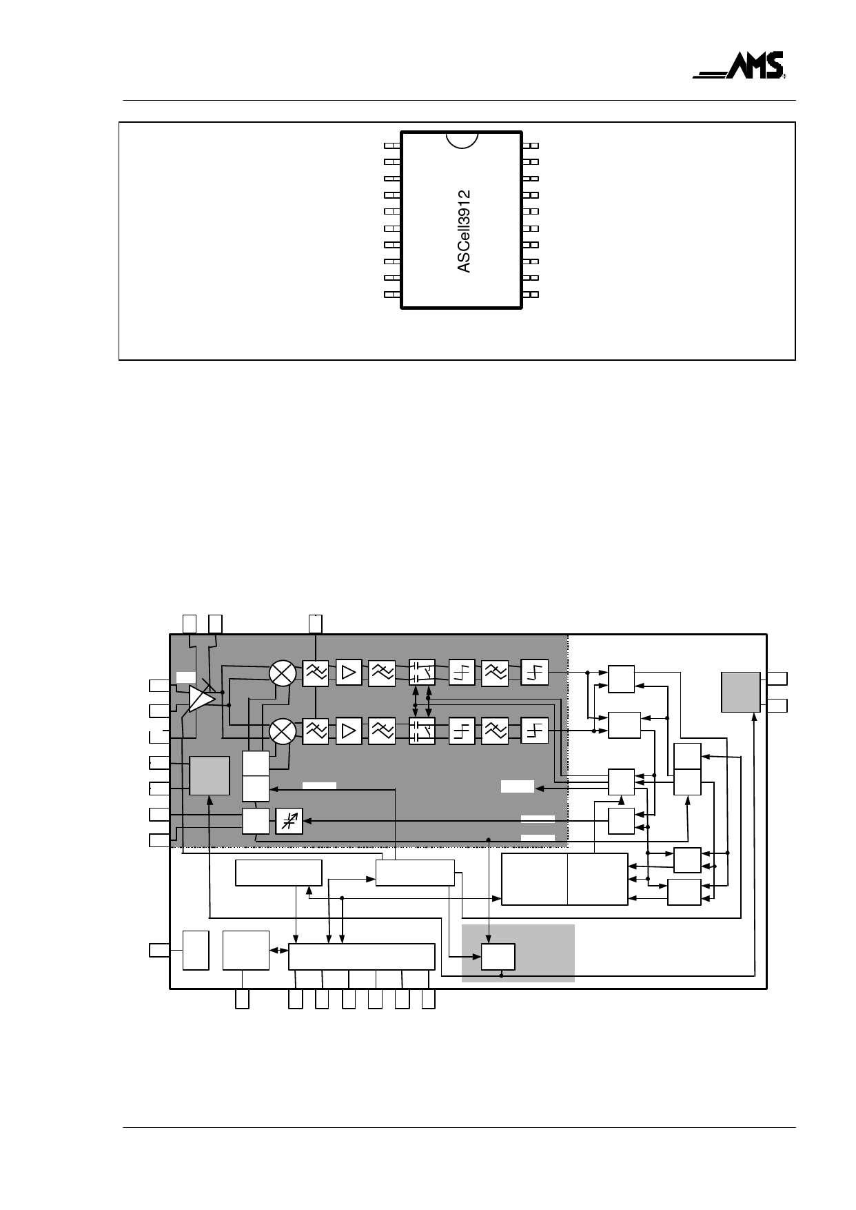
1 Functional Description
The Figure 1 shows the block diagram of the ASCell3912. The analog part of the ASCell3912
consists of a direct conversion receiver, a triple band RF synthesizer and the DC-cancellation.
The digital part includes the burst interference resistant protocol decoder the control logic and
the µC interface.
LC
LC
+
-
G
M
C
RF+
10dB
RF-
RFGND
AVDD
AGND
XTAL+
XTAL-
RF
Power
Supply
90°
OSC
PLL
XO
RF-SEL
LNA
STATE REGISTER
SETUP-
REGISTER
TEST1
Scan
Test
Functional
Test
INTERFACE
TE
µC
_C
RE
_I
W
AK
DN_
DK_
DA
TA
ST
LK
NT
E_
E
CL
2
UP
Figure 1:
Block diagram of the ASCell3912.
RF-Power
I
DEM
Q
∅-Det
DC-Offset
Bandwith CTRL
VDD
Digital
Power
GND
Supply
%
n
CLK
GEN
XOT[3:0]
XO-CLK
AFC
PROTOCOL
DECODER
DATA-
RECOVERY
XO-SEL
FIR
SYNC
1/STR
Sleeptime
control
ASCell3912
Rev. A, February 2000
Page 3 of 14
Share Link: 