ASCELL3912 Просмотр технического описания (PDF) - austriamicrosystems AG
Номер в каталоге
Компоненты Описание
производитель
ASCELL3912 Datasheet PDF : 14 Pages
| |||
ISM 868 MHz, 433 MHz and 315 MHz FSK Receiver Cell – Preliminary Data Sheet
ASCell3912
Austria Mikro Systeme International AG
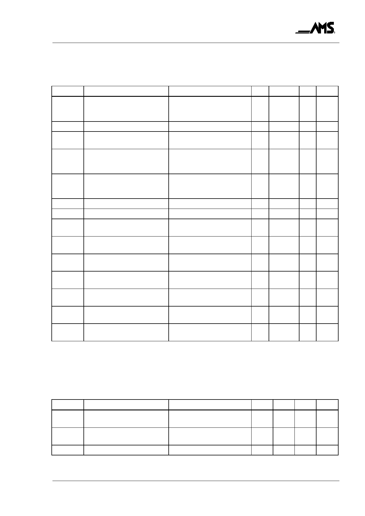
2.3 Receiver Operation
TA = 23 °C, VDD, AVDD = 3.6 V, unless specified otherwise. Devive functional for TA= -40 to
+85 °C.
Symbol Parameter
Conditions / Notes
Min Typ Max
FC
Carrier Frequency
Depends on different external
crystals.
315.000
433.920
868.300
Rin
Input impedance
Capacitive part t.b.d.
200~ 400
?F
Nominal FSK frequency devi a- 315, 433.92, 868.3MHz
61
69
tion
Fxosc
Crystal oscillator (XOSC) fre- 315,000 MHz: max +/- 50ppm
quency
433.920 MHz: max +/- 50ppm
868.300 MHz: max +/-25ppm
19,6875
13.5600
13.5672
TFxosc
Crystal oscillator (XOSC) fre- 315,000 MHz: (-40~+85 °C),
50
quency tolerance
433.920 MHz: (-40~+85 °C),
50
868.300 MHz: (-40~+85 °C).
25
DR,gross
RF
1)
Sens
RFSensT
Gross Data Rate
Including protocol.
Receiver sensitivity
-10 °C<TA<+70 °C
Temperature sensitivity reduc- -40<TA<-10 °C. or
tion
+70>TA>+85 °C.
18.235
-96 -100
4
RFSensFoffim Receiver sensitivity reduction @maximum receiver sensitiv-
7
caused by frequency offset ity reduction @ 44 kHz offset
RFSensLNA
BI200KHz2)
BI1MHz2)
BI10MHz2)
Sensitivity reduction caused
by LNA gain switching
Blocking immunity
200 kHz – 1 MHz
Blocking immunity
1-10 MHz
Blocking immunity @
>10 MHz
Without external filter.
Without external filter
Without external filter
10
0
21
63
PLOfeed
LO @ FC power available at
-28
LC+ and LC- nodes
Units
MHz
MHz
MHz
Ω
kHz
MHz
MHz
MHz
ppm
ppm
ppm
kbps
dBm
dB
dB
dB
dB
dB
dB
dBm
1)
Standard Receive Quality (SRQ): Message reception successfully finished after <80 ms in 80% of all transmission
trails.
2)
CW blocking signal relative to applied useful signal with –94dBm power level and SRQ.
Measured without frequency offset and at +25 °C
Receiver Timing
Symbol
TDni
Parameter
Time to received FSK data
TDwi
Time to received FSK data
Tstop
RX switch off time
Conditions / Notes
Min Typ Max Units
Configured for fast response 27
(receiver sleep time = 0)
80 ms
Using low idle duty cycle the 40
(receiver sleep time >0)
92 ms
Timeout for comfort functions
30
ms
Rev. A, February 2000
Page 10 of 14
Share Link: 