AS1154_V2 Просмотр технического описания (PDF) - austriamicrosystems AG
Номер в каталоге
Компоненты Описание
производитель
AS1154_V2 Datasheet PDF : 16 Pages
| |||
AS1154
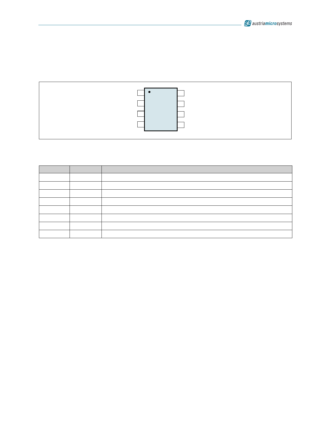
Datasheet - Pinout
4 Pinout
Pin Assignments
Figure 2. Pin Assignments (Top View)
VCC 1
IN1 2
IN2 3
GND 4
AS1154
8 OUT1-
7 OUT1+
6 OUT2+
5 OUT2-
Pin Descriptions
Table 1. Pin Descriptions
Pin Number Pin Name
1
VCC
2
IN1
3
IN2
4
GND
5
OUT2-
6
OUT2+
7
OUT1+
8
OUT1-
Description
Power Supply Input. Bypass VCC to GND with 0.1µF and 0.001µF ceramic capacitors.
LVTTL/LVCMOS Driver Input
LVTTL/LVCMOS Driver Input
Ground
Inverting LVDS Driver Output
Noninverting LVDS Driver Output
Noninverting LVDS Driver Output
Inverting LVDS Driver Output
www.austriamicrosystems.com/Interfaces-LVDS/AS1154
Revision 1.02
2 - 16
Share Link: 