AS1334 Просмотр технического описания (PDF) - austriamicrosystems AG
Номер в каталоге
Компоненты Описание
производитель
AS1334 Datasheet PDF : 19 Pages
| |||
AS1334
Datasheet - Absolute Maximum Ratings
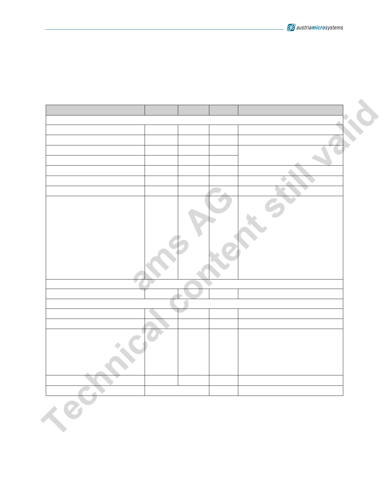
5 Absolute Maximum Ratings
Stresses beyond those listed in Table 2 may cause permanent damage to the device. These are stress ratings only, and functional operation of
the device at these or any other conditions beyond those indicated in Electrical Characteristics on page 4 is not implied. Exposure to absolute
maximum rating conditions for extended periods may affect device reliability.
Table 2. Absolute Maximum Ratings
Parameter
Electrical Parameters
lid VDD, PVIN to SGND
PGND to SGND
POK, EN, FB
a SW
v PVIN to VDD
Input Voltage Range
ill Recommended Load Current
Min
Max
-0.3
-0.3
SGND - 0.3
PGND - 0.3
-0.3
2.7
+7.0
+0.3
VDD + 0.3
PVIN + 0.3
+0.3
5.5
650
AG t st Ambient Temperature (TA) Range
-40
+85
ms ten Electrostatic Discharge
a n Human Body Model
2
o Temperature Ranges and Storage Conditions
c Junction Temperature (TJ-MAX)
+150
Storage Temperature Range
-55
+150
al Package Body Temperature
+260
nic Humidity
Tech Moisture Sensitive Level
5
86
1
Units
Notes
V
V
V
7.0V max
V
V
V
mA
In applications where high power dissipation and/
or poor package thermal resistance is present,
the maximum ambient temperature may have to
be derated.
Maximum ambient temperature (TA-MAX) is
dependent on the maximum operating junction
ºC
temperature (TJ-MAX-OP = 125ºC), the maximum
power dissipation
of the device in the application (PD-MAX), and the
junction-to ambient thermal resistance of the
part/package in the application (θJA), as given by
the following
equation: TA-MAX = TJ-MAX-OP – (θJA × PD-MAX).
kV
Norm: MIL 883 E method 3015
ºC
ºC
The reflow peak soldering temperature (body
temperature) specified is in accordance with IPC/
JEDEC J-STD-020“Moisture/Reflow Sensitivity
ºC
Classification for Non-Hermetic Solid State
Surface Mount Devices”.
The lead finish for Pb-free leaded packages is
matte tin (100% Sn).
%
Non-condensing
Represents a max. floor life time of unlimited
www.austriamicrosystems.com/DC-DC_Step-Down/AS1334
Revision 1.09
3 - 18
Share Link: 