APT7846 Просмотр технического описания (PDF) - Anpec Electronics
Номер в каталоге
Компоненты Описание
производитель
APT7846 Datasheet PDF : 15 Pages
| |||
APT7846
+Vcc
Y+
100kΩ
PENORQ
X+
this method could be used with field programmable
gate arrays (FPGAs) or application specific integrated
circuits (ASICs). (Note that this effectively increases
the maximum conversion rate of the converter).
AC Timing
Figure 12 and Table VI provide detailed timing of
the APT7846.
Y+,Y- Driver
Y-
ON
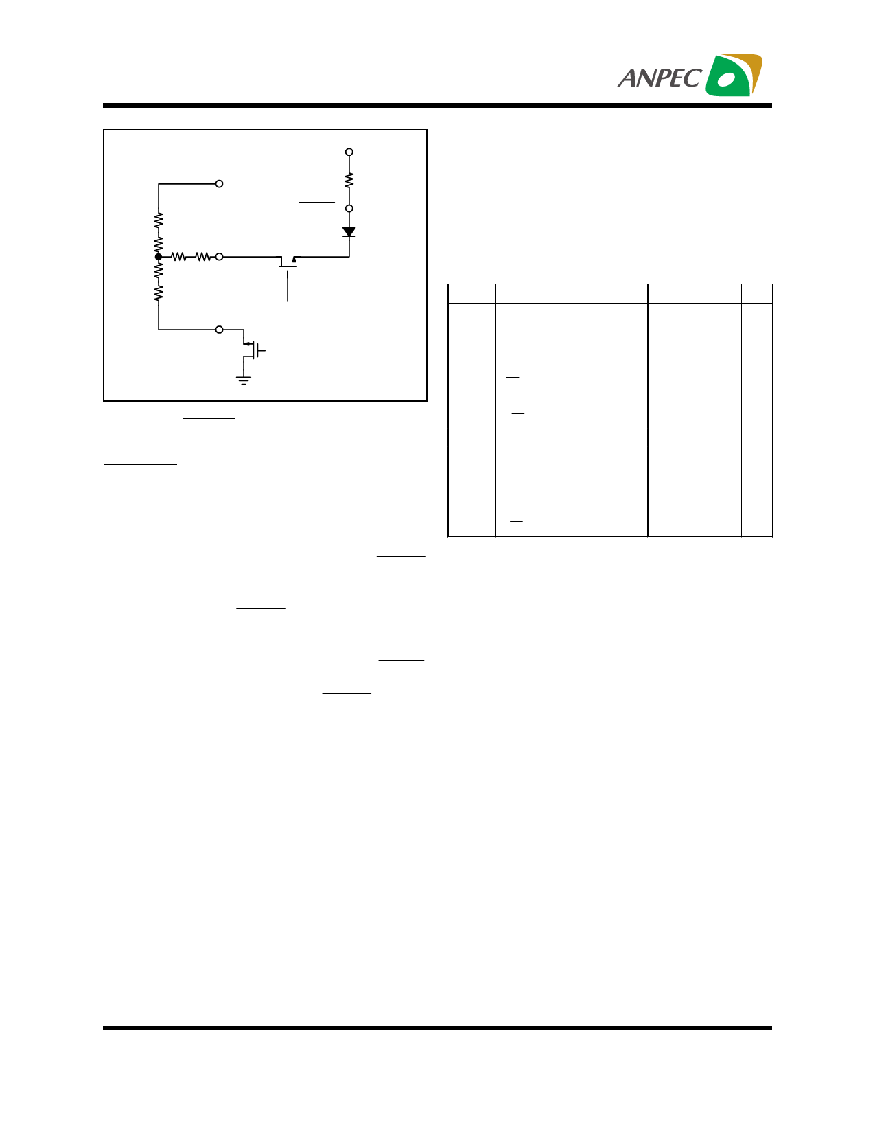
FIGURE 9. PERIRQ Functional Block Diagram
PENIRQ Output
The pen interrupt output function is detailed in Figure
9. By connecting a pull-up resistor to VCC (typically
100kΩ) , the PENIRQ output is HIGH. While in the
power-down mode , with PD0 = PD1 = 0 , the Y
driver is ON and connected to GND and the PENIRQ.
output is connected to the X+ input. When the panel
is touched , the X+ input is pulled to ground through
the touch screen and PENIRQ output goes LOW due
to the current path through the panel to GND , initiat-
ing an interrupt to the processor. During the mea-
surement cycles for X- and Y-Position , the PENIRQ
output diode will be internally connected to GND and
the X+ input disconnected from the PENIRQ diode to
eliminate any leakage current from the pull-up resis-
tor to flow through the touch screen , thus causing no
errors.
SYMBOL
DESCRIPTION
MIN TYP MAX UNIT
tACQ
Acquisition Time
1.5
tDS DIN Valid Prior to DCLK Rising 100
tDH
DIN Hold After DCLK HIGH 10
tDO
DCLK Falling to DOUT Vaild
tDV
CS Falling to DOUT Enabled
tTR
CS Rising to DOUT Disabled
tCSS
CS Falling to DCLK Rising 100
tCSH
CS Rising to DCLK lgnored
0
tCH
DCLK HIGH
200
tCL
DCLK LOW
200
tBD
DCLK Falling to BUSY Rising
tBDV
CS Falling to BUSY Enabled
tBTR
CS Rising to BUSY Disable
µs
ns
ns
200 ns
200 ns
200 ns
ns
ns
ns
ns
200 ns
200 ns
200 ns
TABLE VI. Timing Specifications (+Vcc=+2.7V and
Above , TA=-40°C to +85°C , CLOAD=50pF).
16-Clocks or 15-Clocks per Con-
version
The APT7846 will alow a conversion every 16 clock
cycles , as shown in Figure 10. This figure shows
possible serial communication occurring with other
serial peripherals between each byte transfer be-
tween the processor and the converter.
Figure 11 provides the fastest way to clock the
APT7846. This method will not work with the serial
interface of most microcontrollers and digital signal
processors as they are generally not capable of pro-
viding 15 clock cycles per serial transfer. However ,
Copyright ANPEC Electronics Corp.
11
Rev. A.6 - Dec., 2001
www.anpec.com.tw
Share Link: 