HM-6617/883 Просмотр технического описания (PDF) - Intersil
Номер в каталоге
Компоненты Описание
производитель
HM-6617/883 Datasheet PDF : 7 Pages
| |||
HM-6617/883
Absolute Maximum Ratings
Thermal Information
Supply Voltage . . . . . . . . . . . . . . . . . . . . . . . . . . . . . . . . . . . . . +7.0V
Input, Output or I/O Voltage . . . . . . . . . . . GND -0.3V to VCC +0.3V
Typical Derating Factor . . . . . . . . . . . . 5mA/MHz Increase in ICCOP
ESD Classification . . . . . . . . . . . . . . . . . . . . . . . . . . . . . . . . Class 1
Operating Conditions
Operating Voltage Range . . . . . . . . . . . . . . . . . . . . . +4.5V to +5.5V
Operating Temperature Range . . . . . . . . . . . . . . . . -55oC to +125oC
Input Low Voltage . . . . . . . . . . . . . . . . . . . . . . . . . . . . -0.3V to +0.8V
Input High Voltage . . . . . . . . . . . . . . . . . . . . . . +2.4V to VCC +0.3V
Thermal Resistance
SBDIP Package . . . . . . . . . . . . . . . . . .
48θoJCA/W
9oθCJC/W
Maximum Storage Temperature Range . . . . . . . . .-65oC to +150oC
Maximum Junction Temperature . . . . . . . . . . . . . . . . . . . . . . +175oC
Maximum Lead Temperature (Soldering 10s) . . . . . . . . . . . . +300oC
Die Characteristics
Gate Count . . . . . . . . . . . . . . . . . . . . . . . . . . . . . . . . . . . 5473 Gates
CAUTION: Stresses above those listed in “Absolute Maximum Ratings” may cause permanent damage to the device. This is a stress only rating and operation of
the device at these or any other conditions above those indicated in the operational sections of this specification is not implied.
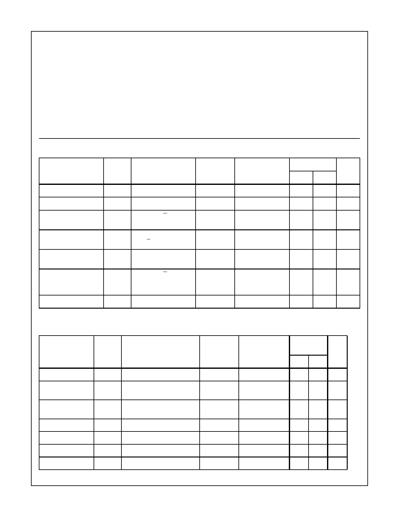
TABLE 1. HM-6617/883 DC ELECTRICAL PERFORMANCE SPECIFICATIONS
Device Guaranteed and 100% Tested
PARAMETER
SYMBOL
(NOTES 1, 4)
CONDITIONS
GROUP A
SUBGROUPS
TEMPERATURE
LIMITS
MIN MAX
High Level Output Voltage VOH1 VCC = 4.5V, IO = -2.0mA
1, 2, 3
-55oC ≤ TA ≤ +125oC 2.4
-
Low Level Output Voltage VOL VCC = 4.5V, IO = +4.8mA
1, 2, 3
-55oC ≤ TA ≤ +125oC
-
0.4
High Impedance Output
Leakage Current
IIOZ VCC = 5.5V, G = 5.5V,
VI/O = GND or VCC
1, 2, 3
-55oC ≤ TA ≤ +125oC -1.0
1.0
Input Leakage Current
II
VCC = 5.5V, VI = GND or
VCC, P Not Tested
1, 2, 3
-55oC ≤ TA ≤ +125oC -1.0
1.0
Standby Supply Current
ICCSB VI = VCC or GND,
VCC = 5.5V, IO = 0mA
1, 2, 3
-55oC ≤ TA ≤ +125oC
-
100
Operating Supply Current ICCOP VCC = 5.5V, G = GND,
1, 2, 3
-55oC ≤ TA ≤ +125oC
-
20
(Note 3), f = 1MHz, IO =
0mA, VI = VCC or GND
Functional Test
FT VCC = 4.5V (Note 6)
7, 8A, 8B -55oC ≤ TA ≤ +125oC
-
-
UNITS
V
V
µA
µA
µA
mA
TABLE 2. HM-6617/883 AC ELECTRICAL PERFORMANCE SPECIFICATIONS
Device Guaranteed and 100% Tested
PARAMETER SYMBOL
(NOTES 1, 2, 4)
CONDITIONS
GROUP A
SUBGROUPS
TEMPERATURE
LIMITS
HM-6617/883
MIN MAX UNITS
Address Access Time TAVQV VCC = 4.5V and 5.5V (Note 5)
9, 10, 11
-55oC ≤ TA ≤ +125oC -
140
ns
Output Enable Access
Time
TGLQV VCC = 4.5V and 5.5V
9, 10, 11
-55oC ≤ TA ≤ +125oC -
50
ns
Chip Enable Access
Time
TELQV VCC = 4.5V and 5.5V
9, 10, 11
-55oC ≤ TA ≤ +125oC -
120
ns
Address Setup Time
TAVEL VCC = 4.5V and 5.5V
9, 10, 11
-55oC ≤ TA ≤ +125oC 20
-
ns
Address Hold Time
TELAX VCC = 4.5V and 5.5V
9, 10, 11
-55oC ≤ TA ≤ +125oC 25
-
ns
Chip Enable Low Width TELEH VCC = 4.5V and 5.5V
9, 10, 11
-55oC ≤ TA ≤ +125oC 120
-
ns
Chip Enable High Width TEHEL VCC = 4.5V and 5.5V
9, 10, 11
-55oC ≤ TA ≤ +125oC 40
-
ns
3
Share Link: 