RF1K4915496 Просмотр технического описания (PDF) - Intersil
Номер в каталоге
Компоненты Описание
производитель
RF1K4915496 Datasheet PDF : 8 Pages
| |||
RF1K49154
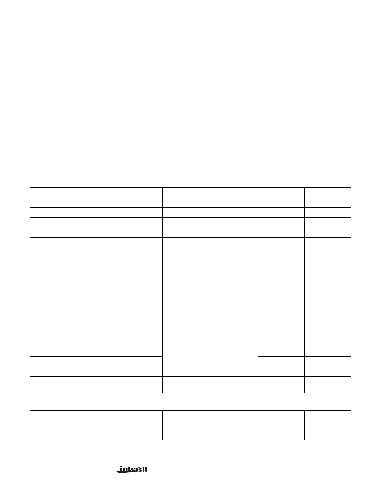
Absolute Maximum Ratings TA = 25oC, Unless Otherwise Specified
Drain to Source Voltage (Note 1) . . . . . . . . . . . . . . . . . . . . . . . . . . . . . . . . . . . . . .VDSS
Drain to Gate Voltage (RGS = 20kΩ, Note 1) . . . . . . . . . . . . . . . . . . . . . . . . . . . . VDGR
Gate to Source Voltage . . . . . . . . . . . . . . . . . . . . . . . . . . . . . . . . . . . . . . . . . . . . . .VGS
Drain Current Continuous (Pulse width = 5s) . . . . . . . . . . . . . . . . . . . . . . . . . . . . . . ID
Pulsed (Figure 5) . . . . . . . . . . . . . . . . . . . . . . . . . . . . . . . . . . . . . . . . . . . . . . . . . IDM
Pulsed Avalanche Rating (Figure 6) . . . . . . . . . . . . . . . . . . . . . . . . . . . . . . . . . . . . EAS
Power Dissipation . . .
Derate Above 25oC
.
.
.
.
.
.
.
.
.
.
.
.
.
.
.
.
.
.
.
.
.
.
.
.
.
.
.
.
.
.
.
.
.
.
.
.
.
.
.
.
.
.
.
.
.
.
.
.
.
.
.
.
.
.
.
.
.
.
.
.
.
.
.
.
.
.
.
.
.
.
.
.
.
.
.
.
.
.
.
.
.
.
.
.
.
.
.
.
.
.
.
.
.
.
.
.
PD
..
Operating and Storage Temperature . . . . . . . . . . . . . . . . . . . . . . . . . . . . . . . . TJ, TSTG
Maximum Temperature for Soldering
Leads at 0.063in (1.6mm) from Case for 10s. . . . . . . . . . . . . . . . . . . . . . . . . . . . . TL
Package Body for 10s, See Techbrief 334 . . . . . . . . . . . . . . . . . . . . . . . . . . . . . Tpkg
RF1K49154
60
60
±20
2
Refer to Peak Current Curve
Refer to UIS Curve
2
0.016
-55 to 150
300
260
UNITS
V
V
V
A
W
W/oC
oC
oC
oC
CAUTION: Stresses above those listed in “Absolute Maximum Ratings” may cause permanent damage to the device. This is a stress only rating and operation of the
device at these or any other conditions above those indicated in the operational sections of this specification is not implied.
NOTE:
1. TJ = 25oC to 125oC.
Electrical Specifications TA = 25oC, Unless Otherwise Specified
PARAMETER
SYMBOL
TEST CONDITIONS
Drain to Source Breakdown Voltage
Gate Threshold Voltage
BVDSS
VGS(TH)
ID = 250µA, VGS = 0V, (Figure 12)
VGS = VDS, ID = 250µA, (Figure 11)
Zero Gate Voltage Drain Current
Gate to Source Leakage Current
Drain to Source On Resistance
Turn-On Time
Turn-On Delay Time
Rise Time
Turn-Off Delay Time
Fall Time
IDSS
IGSS
rDS(ON)
tON
td(ON)
tr
td(OFF)
tf
VDS = 55V, VGS = 0V
VDS = 50V, VGS = 0V, TC = 150oC
VGS = ±20V
ID = 2A, VGS = 10V, (Figures 9, 10)
VDD = 30V, ID ≈ 2A,
RL = 15Ω, VGS = 10V,
RGS = 25Ω
(Figure 14)
Turn-Off Time
Total Gate Charge
Gate Charge at 10V
Threshold Gate Charge
Input Capacitance
Output Capacitance
Reverse Transfer Capacitance
Thermal Resistance Junction to Ambient
tOFF
Qg(TOT)
Qg(10)
Qg(TH)
CISS
COSS
CRSS
RθJA
VGS = 0V to 20V
VGS = 0V to 10V
VGS = 0V to 2V
VDD = 48V,
ID = 2A,
RL = 24Ω
(Figure 14)
VDS = 25V, VGS = 0V,
f = 1MHz (Figure 13)
Pulse Width = 1s
Device Mounted on FR-4 Material
MIN
TYP
MAX UNITS
60
-
-
V
2
-
4
V
-
-
1
µA
-
-
250
µA
-
-
±10
µA
-
-
0.130
Ω
-
-
50
ns
-
10
-
ns
-
25
-
ns
-
70
-
ns
-
35
-
ns
-
-
155
ns
-
26
32
nC
-
14
17
nC
-
0.8
1.0
nC
-
340
-
pF
-
140
-
pF
-
40
-
pF
-
-
62.5
oC/W
Source to Drain Diode Specifications
PARAMETER
Source to Drain Diode Voltage
Reverse Recovery Time
SYMBOL
TEST CONDITIONS
VSD
ISD = 2A
trr
ISD = 2A, dISD/dt = 100A/µs
MIN
TYP
MAX UNITS
-
-
1.5
V
-
-
62
ns
2
Share Link: 