MAX1246BCPE Просмотр технического описания (PDF) - Maxim Integrated
Номер в каталоге
Компоненты Описание
производитель
MAX1246BCPE Datasheet PDF : 25 Pages
| |||
+2.7V, Low-Power, 4-Channel,
Serial 12-Bit ADCs in QSOP-16
TIMING CHARACTERISTICS
(VDD = +2.7V to +3.6V (MAX1246); VDD = +2.7V to +5.25V (MAX1247); TA = TMIN to TMAX; unless otherwise noted.)
PARAMETER
SYMBOL
CONDITIONS
MIN TYP
Acquisition Time
tACQ
1.5
DIN to SCLK Setup
tDS
100
DIN to SCLK Hold
tDH
MAX124_ _C/E
20
SCLK Fall to Output Data Valid
tDO Figure 1
MAX124_ _M
20
CS Fall to Output Enable
tDV Figure 1
CS Rise to Output Disable
tTR Figure 2
CS to SCLK Rise Setup
tCSS
100
CS to SCLK Rise Hold
tCSH
0
SCLK Pulse Width High
tCH
200
SCLK Pulse Width Low
tCL
200
SCLK Fall to SSTRB
tSSTRB Figure 1
CS Fall to SSTRB Output Enable
tSDV External clock mode only, Figure 1
CS Rise to SSTRB Output Disable tSTR External clock mode only, Figure 2
SSTRB Rise to SCLK Rise
tSCK Internal clock mode only (Note 7)
0
MAX
0
200
240
240
240
240
240
240
UNITS
µs
ns
ns
ns
ns
ns
ns
ns
ns
ns
ns
ns
ns
ns
Note 1: Tested at VDD = 2.7V; COM = 0V; unipolar single-ended input mode.
Note 2: Relative accuracy is the deviation of the analog value at any code from its theoretical value after the full-scale range has
been calibrated.
Note 3: MAX1246—internal reference, offset nulled; MAX1247—external reference (VREF = +2.500V), offset nulled.
Note 4: Ground “on” channel; sine wave applied to all “off” channels.
Note 5: Conversion time defined as the number of clock cycles multiplied by the clock period; clock has 50% duty cycle.
Note 6: The common-mode range for the analog inputs is from AGND to VDD.
Note 7: Guaranteed by design. Not subject to production testing.
Note 8: External load should not change during conversion for specified accuracy.
Note 9: ADC performance is limited by the converter’s noise floor, typically 300µVp-p.
| | Note 10: Measured as VFS(2.7V) - VFS(VDD.MAX) .
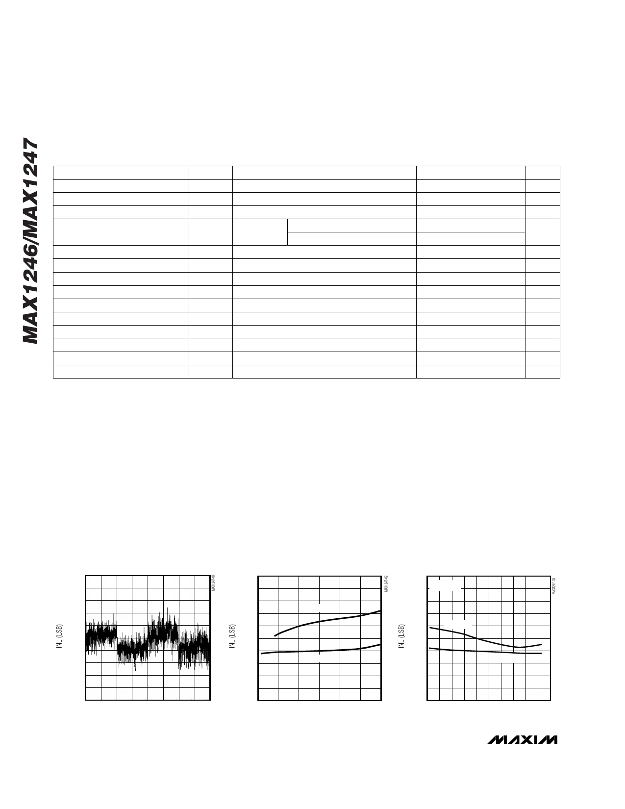
__________________________________________Typical Operating Characteristics
(VDD = 3V, VREF = 2.5V, fSCLK = 2MHz, CLOAD = 20pF, TA = +25°C, unless otherwise noted.)
0.5
0.4
0.3
0.2
0.1
0
-0.1
-0.2
-0.3
-0.4
-0.5
0
INTEGRAL NONLINEARITY
vs. CODE
1024
2048
3072
4096
CODE
INTEGRAL NONLINEARITY
vs. SUPPLY VOLTAGE
0.50
0.45
0.40
MAX1246
0.35
0.30
0.25
0.20
MAX1247
0.15
0.10
0.05
0.00
2.25 2.75 3.25 3.75 4.25 4.75 5.25
VDD (V)
INTEGRAL NONLINEARITY
vs. TEMPERATURE
0.50
0.45 VDD = 2.7V
0.40
0.35
0.30
MAX1246
0.25
0.20
0.15
MAX1247
0.10
0.05
0.00
-60
-20 20
60 100 140
TEMPERATURE (°C)
6 _______________________________________________________________________________________
Share Link: 