AP393 Просмотр технического описания (PDF) - Diodes Incorporated.
Номер в каталоге
Компоненты Описание
производитель
AP393 Datasheet PDF : 15 Pages
| |||
AP393
LOW POWER LOW OFFSET VOLTAGE DUAL
COMPARATORS
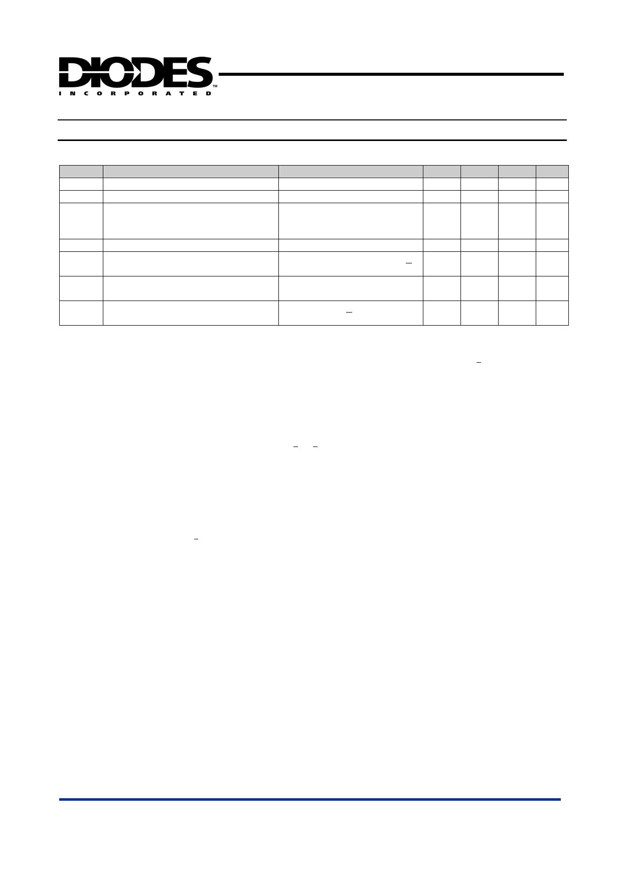
Electrical Characteristics ( VCC = 5V ) ( Note 7 )
Symbol
Parameter
Conditions
VOFFSET Input Offset Voltage
(Note 12)
IOFFSET Input Offset Current
IIN(+) -IIN(-), VCM = 0V
IIN(+) or IIN(-) with Output In
IBIAS Input Bias Current
Linear Range, VCM = 0V
(Note 8)
Input Common Mode Voltage Range V+ =30V (Note 9)
VSAT Saturation Voltage
VIN(-) = 1V, VIN(+) = 0, ISINK <
4mA
IO(Leak) Output Leakage Current
Differential Input Voltage
VIN(-) = 0, VIN(+) = 1V,
VO = 30V
Keep All VIN’s > 0V (or V-, if
Used), (Note 11)
Min.
-
-
-
0
-
-
-
Typ. Max. Unit
-
9 mV
-
150 nA
-
400 nA
- V+ -2.0 V
-
700 mV
-
1.0 µA
-
36 V
Note:
4. For operating at high temperatures, the AP393 must be derated based on a 125°C maximum junction temperature and a
thermal resistance of 170°C/W which applies for the device soldered in a printed circuit board, operating in a still air ambient.
The low bias dissipation and the “ON-OFF” characteristic of the outputs keeps the chip dissipation very small (PD <100mW), provided the
output transistors are allowed to saturate.
5. Short circuits from the output to V+ can cause excessive heating and eventual destruction. When considering short circuits to
ground, the maximum output current is approximately 20mA independent of the magnitude of V+.
6. This input current will only exist when the voltage at any of the input leads is driven negative. It is due to the collector-base
junction of the input PNP transistors becoming forward biased and thereby acting as input diode clamps. In addition to this
diode action, there is also lateral NPN parasitic transistor action on the IC chip. This transistor action can cause the output
voltages of the comparators to go to the V+ voltage level (or to ground for a large overdrive) for the time duration that an input
is driven negative. This is not destructive and normal output states will re-establish when the input voltage, which is negative,
again returns to a value greater than -0.3V.
7. The AP393 temperature specifications are limited to 0°C < TOP < +70°C.
8. The direction of the input current is out of the IC due to the PNP input stage. This current is essentially constant, independent
of the state of the output so no loading change exists on the reference or input lines.
9. The input common-mode voltage or either input signal voltage should not be allowed to go negative by more than 0.3V. The
upper end of the common-mode voltage range is V+-1.5V at 25°C, but either or both inputs can go to 36V without damage,
independent of the magnitude of V+.
10. The response time specified is for a 100mV input step with 5mV overdrive. For larger overdrive signals 300ns can be
obtained, see typical performance characteristics section.
11. Positive excursions of input voltage may exceed the power supply level. As long as the other voltage remains within the
common-mode range, the comparator will provide a proper output state. The low input voltage state must not be less than
-0.3V (or 0.3V below the magnitude of the negative power supply, if used).
12. At output switch point, VO ~ 1.4V, RS=0Ω with V+ from 5V to 30V; and over the full input common-mode range (0V to V+-1.5V),
at 25°C.
13. Refer to RETS193AX for AP393 military specifications.
AP393 Rev. 3
5 of 15
www.diodes.com
FEBRUARY 2007
© Diodes Incorporated
Share Link: 