AP3019A Просмотр технического описания (PDF) - BCD Semiconductor
Номер в каталоге
Компоненты Описание
производитель
AP3019A Datasheet PDF : 15 Pages
| |||
Data Sheet
WHITE LED STEP-UP CONVERTER
AP3019A
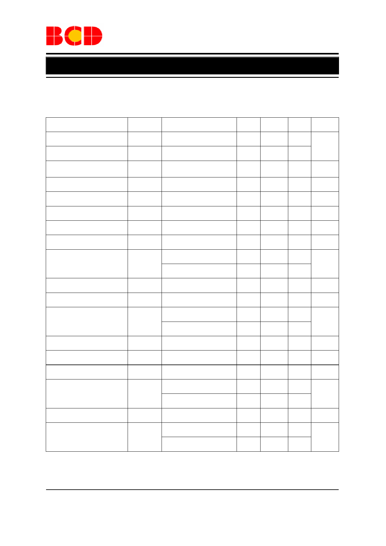
Electrical Characteristics
VIN =3V, VCTRL=3V, TA =25°C, unless otherwise specified.
Parameter
Symbol
Conditions
Minimum Operating Voltage
Maximum Operating Voltage
Feedback Voltage (Note 2)
FB Pin Bias Current
Quiescent Current
Shutdown Quiescent Current
Switching Frequency
VIN (min)
VIN (max)
VFB
IFB
IOUT=20mA, 4 LEDs,
TA=-40oC to 85oC
IQ
VFB=VIN, no switching
ISHDN
VCTRL=0V
f
Maximum Duty Cycle
Switch Current Limit (Note 3)
DMAX
ILIMIT
D=40%
D=80%
Switch VCE Saturation Voltage
Switch Leakage Current
CTRL Pin Voltage
VCESAT
VCTRL
ISW=250mA
VSW=5V
High
low
CTRL Pin Bias Current
OVP Voltage
Schottky Forward Drop
Schottky Leakage Current
Soft Start Time
ICTRL
VOV
VDROP
t
ID=150mA
VR(reverse voltage)=23V
VR(reverse voltage)=27V
Thermal Resistance
(Junction to Case)
SOT-23-6
θJC
TSOT-23-6
Min
2.5
188
1.5
2.0
0.9
90
1.8
Typ
200
35
2.5
4.0
1.2
93
550
550
360
0.01
100
30
0.7
0.1
300
60
60
Max Unit
V
16
212
mV
100
nA
3.2
mA
6.0
µA
1.5 MHz
%
mA
mV
5
µA
V
0.5
µA
V
V
4
µA
150
µS
°C/W
Note 2: The bold type specifications of full temperature range are guaranteed by design (GBD).
Note 3: The switch current limit is related to duty cycle. Please refer to Figure 15 for detail.
Mar. 2010 Rev. 1.7
BCD Semiconductor Manufacturing Limited
5
Share Link: 