AO4612 Просмотр технического описания (PDF) - Unspecified
Номер в каталоге
Компоненты Описание
производитель
AO4612 Datasheet PDF : 9 Pages
| |||
AO4612
60V Complementary Enhancement
Mode Field Effect Transistor
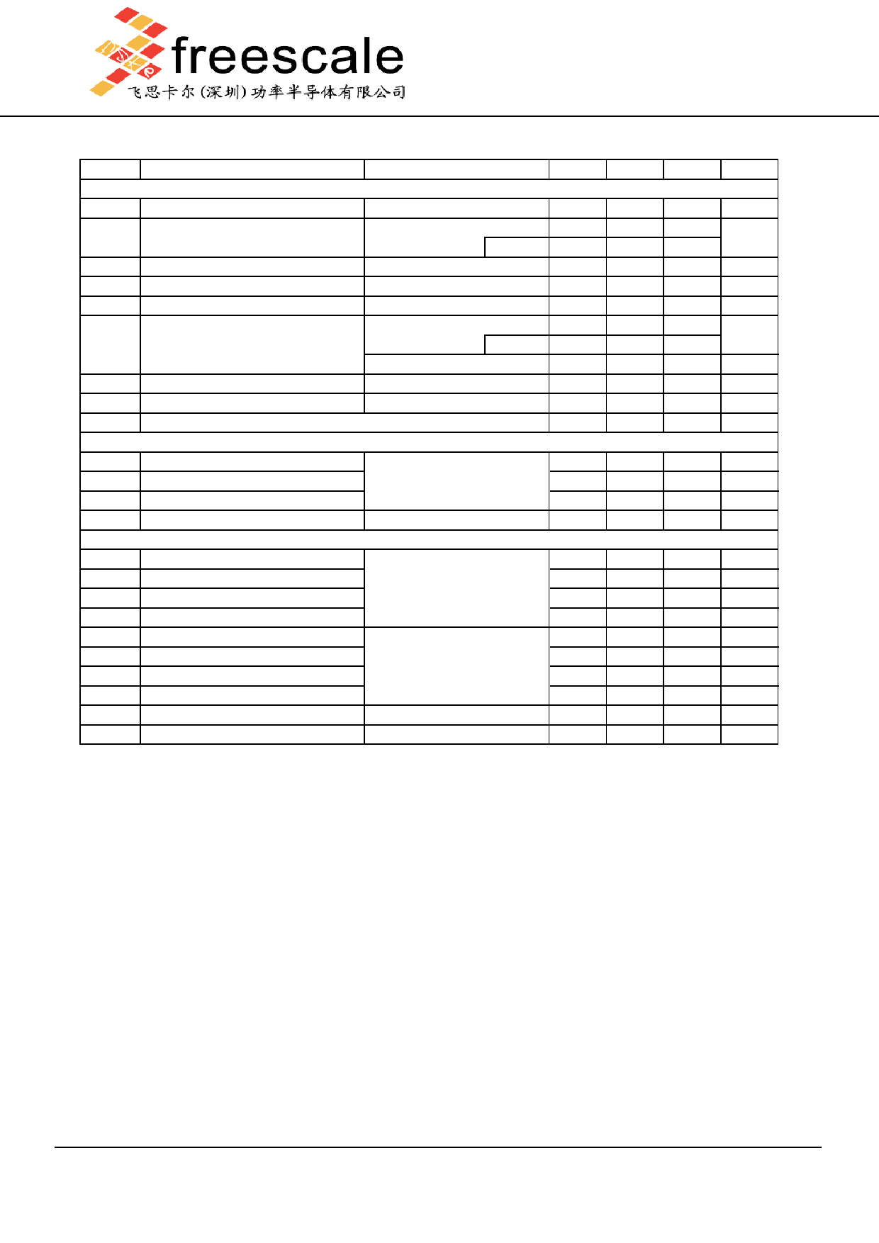
N Channel Electrical Characteristics (TJ=25°C unless otherwise noted)
Symbol
Parameter
Conditions
Min
Typ
Max Units
STATIC PARAMETERS
BVDSS Drain-Source Breakdown Voltage
ID=250µA, VGS=0V
60
V
IDSS
Zero Gate Voltage Drain Current
VDS=48V, VGS=0V
TJ=55°C
1
µA
5
IGSS
Gate-Body leakage current
VDS=0V, VGS= ±20V
100
nA
VGS(th) Gate Threshold Voltage
VDS=VGS ID=250µA
1
2.1
3
V
ID(ON)
On state drain current
VGS=10V, VDS=5V
20
A
RDS(ON) Static Drain-Source On-Resistance
VGS=10V, ID=4.5A
TJ=125°C
46
56
mΩ
79
VGS=4.5V, ID=3A
64
77
mΩ
gFS
Forward Transconductance
VDS=5V, ID=4.5A
11
S
VSD
Diode Forward Voltage
IS=1A,VGS=0V
0.74
1
V
IS
Maximum Body-Diode Continuous Current
3
A
DYNAMIC PARAMETERS
Ciss
Input Capacitance
Coss
Output Capacitance
Crss
Reverse Transfer Capacitance
Rg
Gate resistance
VGS=0V, VDS=30V, f=1MHz
VGS=0V, VDS=0V, f=1MHz
450
540
pF
60
pF
25
pF
1.65
2
Ω
SWITCHING PARAMETERS
Qg(10V) Total Gate Charge
8.5
10.5
nC
Qg(4.5V) Total Gate Charge
Qgs
Gate Source Charge
VGS=10V, VDS=30V, ID=4.5A
4.3
5.5
nC
1.6
nC
Qgd
Gate Drain Charge
2.2
nC
tD(on)
Turn-On DelayTime
4.7
7
ns
tr
Turn-On Rise Time
VGS=10V, VDS=30V, RL=6.7Ω,
2.3
4.5
ns
tD(off)
Turn-Off DelayTime
RGEN=3Ω
15.7
24
ns
tf
Turn-Off Fall Time
1.9
4
ns
trr
Body Diode Reverse Recovery Time IF=4.5A, dI/dt=100A/µs
27.5
35
ns
Qrr
Body Diode Reverse Recovery Charge IF=4.5A, dI/dt=100A/µs
32
nC
A: The value of R θJA is measured with the device mounted on 1in 2 FR-4 board with 2oz. Copper, in a still air environment with T A=25°C. The value in
any a given application depends on the user's specific board design. The current rating is based on the t ≤ 10s thermal resistance rating.
B: Repetitive rating, pulse width limited by junction temperature.
C. The R θJA is the sum of the thermal impedence from junction to lead R θJL and lead to ambient.
D. The static characteristics in Figures 1 to 6 are obtained using 80 µs pulses, duty cycle 0.5% max.
E. These tests are performed with the device mounted on 1 in 2 FR-4 board with 2oz. Copper, in a still air environment with T A=25°C. The SOA curve
provides a single pulse rating. Rev3: Oct 2010
2/9
www.freescale.net.cn
Share Link: 