AN7196Z Просмотр технического описания (PDF) - Panasonic Corporation
Номер в каталоге
Компоненты Описание
производитель
AN7196Z Datasheet PDF : 12 Pages
| |||
AN7196Z
ICs for Audio Common Use
s Technical Information (continued)
[2] Application note (continued)
2. Oscillation countermeasures
1) In order to increase the oscillation allowance, connect a capacitor and
a resistor in series between each output terminal and GND as shown
in figure 2.
2) The use of polyester film capacitor having a little fluctuation with
temperature and frequency is recommended as the 0.1 µF capacitor
for oscillation prevention.
1
2,4
13,15
To speaker
0.1 µF
2.2 Ω
3,14
3. Input terminal
Figure 2
1) The reference voltage of input terminal is 0 V. When the input signal has a reference voltage other than 0 V
potential, connect a coupling capacitor (of about several µF) for DC component cut in series with the input
terminal. Check the low-pass frequency characteristics to determine the capacitor value.
2) 10 kΩ or less of signal source impedance Rg can reduce the output end noise voltage.
3) The output offset voltage fluctuates when the signal source impedance Rg is changed. A care must be taken
when using the circuit by directly connecting the volume to the input terminal. In such a case, the use of
coupling capacitor is recommended.
4) If a high frequency signal from tuners enters the input terminal as noise, insert a capacitor of approx. 0.01 µF
between the input terminal and input GND.
When a high frequency signal is inputted, malfunction in protective circuits may occur.
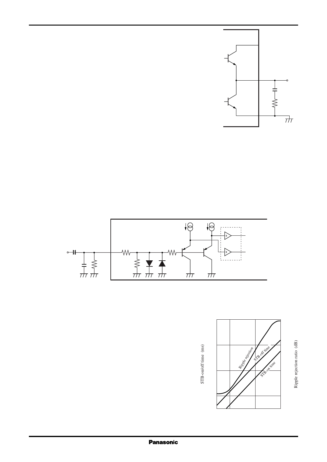
15 µA 15 µA
1 µF
Input signal
0.01 µF
6 200 Ω
4.7 kΩ 11
30 kΩ
400 Ω
To power
Attenuator
4. Ripple filter
Figure 3
1) In order to suppress the fluctuation of supply voltage, connect a capacitor of approx. 33 µF between RF
terminal (pin12) and GND.
2) Relation between RR (Ripple Rejection Ratio) and a capacitor
The larger the capacitance of the ripple filter is, the better the
ripple rejection becomes.
3) Relation between the rise time of circuit and a capacitor
The larger the capacitance of the ripple filter is, the longer the 1 000
time from the power on (standby high) to the sound release
becomes.
60
STB-off time
4) The DC voltage of output terminal is approximately the middle
100
50
point of the ripple filter terminal voltage.
5) The internal circuit of ripple filter terminal is as shown in fig-
ure 5 and the charge current is approx. 3 mA to 10 mA.
10
40
6) The muting circuit turns on when the ripple filter terminal is
VCC − 4 VBE or less.
For that reason, abnormal sound due to waveform distortion at
rising and falling of the circuit is not released.
1.0
10
100
RF capacitor capacitance value (µF)
Figure 4
8
Share Link: 