AMD-X5-133 Просмотр технического описания (PDF) - Advanced Micro Devices
Номер в каталоге
Компоненты Описание
производитель
AMD-X5-133 Datasheet PDF : 67 Pages
| |||
AMD
PRELIMINARY
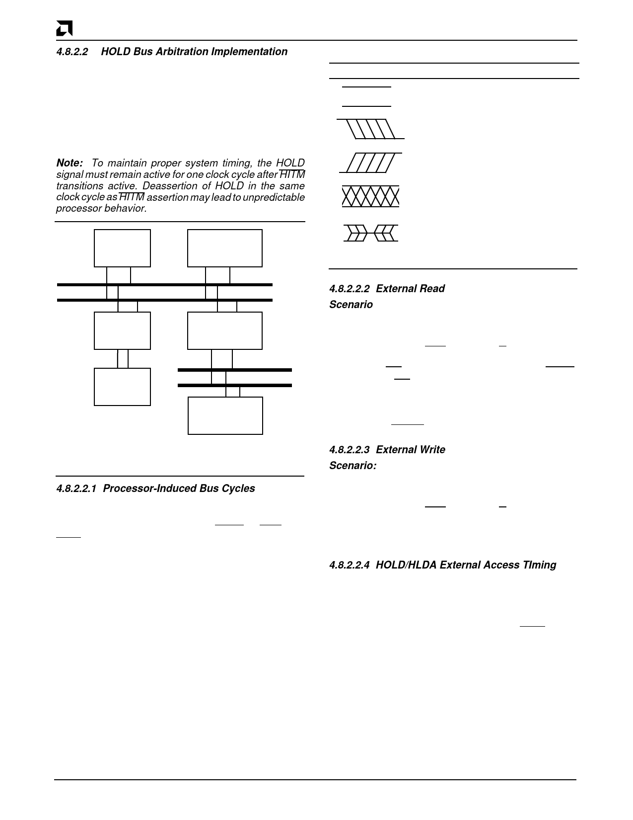
4.8.2.2 HOLD Bus Arbitration Implementation
.
Table 6. Key to Switching Waveforms
The HOLD/HLDA bus arbitration scheme is used prima-
rily in systems where all memory transfers are seen by
the microprocessor. The HOLD/HLDA bus arbitration
scheme permits simple write-back cache design while
maintaining a relatively high performing system. Figure
3 shows a typical system block diagram for HOLD/HLDA
bus arbitration.
Waveform
Inputs
Outputs
Must be steady Will be steady
May change from Will change
H to L
from H to L
Note: To maintain proper system timing, the HOLD
signal must remain active for one clock cycle after HITM
transitions active. Deassertion of HOLD in the same
clock cycle as HITM assertion may lead to unpredictable
processor behavior.
CPU
Local Bus
Peripheral
May change from Will change
L to H
from L to H
Don’t care; any Changing;
change permitted state unknown
Does not apply
Center line is
High-impedance
“Off” state
Address Bus
Data Bus
L2 Cache
I/O Bus
Interface
DRAM
Address Bus
Data Bus
Slow
Peripheral
Figure 3. Typical System Block Diagram
for HOLD/HLDA Bus Arbitration
4.8.2.2.1 Processor-Induced Bus Cycles
In the following scenarios, read accesses are assumed
to be cache line fills. The cases also assume that the
core system logic does not return BRDY or RDY until
HITM is sampled. The addition of wait states follows the
standard 486 bus protocol. For demonstration purpos-
es, only the zero wait state approach is shown. Table 6
explains the key to switching waveforms.
4.8.2.2.2 External Read
Scenario: The data resides in external memory (see
Figure 4).
Step 1 The processor starts the external read access
by asserting ADS = 0 and W/R = 0.
Step 2 WB/WT is sampled in the same cycle as BRDY.
If WB/WT = 1, the data resides in a write-back
cacheable memory location.
Step 3 The processor completes its burst read and as-
serts BLAST.
4.8.2.2.3 External Write
Scenario: The data is written to the external memory
(see Figure 5).
Step 1 The processor starts the external write access
by asserting ADS = 0 and W/R = 1.
Step 2 The processor completes its write to the core
system logic.
4.8.2.2.4 HOLD/HLDA External Access TIming
In systems with two or more bus masters, each bus
master is equipped with individual HOLD and HLDA con-
trol signals. These signals are then centralized to the
core system logic that controls individual bus masters,
depending on bus request signals and the HITM signal.
22
Am5X86 Microprocessor
Share Link: 