AMD-X5-133 Просмотр технического описания (PDF) - Advanced Micro Devices
Номер в каталоге
Компоненты Описание
производитель
AMD-X5-133 Datasheet PDF : 67 Pages
| |||
PRELIMINARY
AMD
If the PWT signal is 0, the external WB/WT signal de-
termines the new state of the line. If the WB/WT signal
was asserted to 1 during reload, the line transits to the
exclusive state. If the WB/WT signal was 0, the line
transits to the shared state. If the PWT signal is 1, it
overrides the WB/WT signal, forcing the line into the
shared state. Therefore, if paging is enabled, the soft-
ware programmed PWT bit can override the hardware
signal WB/WT.
Until the line is reallocated, a write is the only processor
action that can change the state of the line. If the write
occurs to a line in the exclusive state, the data is simply
written into the cache and the line state is changed to
modified. The modified state indicates that the contents
of the line require copy-back to the main memory before
the line is reallocated.
If the write occurs to a line in the shared state, the cache
performs a write of the data on the external bus to update
the external memory. The line remains in the shared
state until it is replaced with a new cache line or until it
is flushed. In the modified state, the processor continues
to write the line without any further external actions or
state transitions.
If the PWT or PCD bits are changed for a specified mem-
ory location, the tag bits in the cache are assumed to
be correct. To avoid memory inconsistencies with re-
spect to cacheability and write status, a cache copy-
back and invalidation should be invoked either by using
the WBINVD instruction or asserting the FLUSH signal.
4.8.2 Snooping Actions and State Transitions
To maintain cache coherency, the CPU must allow
snooping by the current bus master. The bus master
initiates a snoop cycle to check whether an address is
cached in the internal cache of the microprocessor. A
snoop cycle differs from any other cycle in that it is ini-
tiated externally to the microprocessor, and the signal
for beginning the cycle is EADS instead of ADS. The
address bus of the microprocessor is bidirectional to
allow the address of the snoop to be driven by the sys-
tem. A snoop access can begin during any hold state:
s While HOLD and HLDA are asserted
s While BOFF is asserted
s While AHOLD is asserted
In the clock in which EADS is asserted, the micropro-
cessor samples the INV input to qualify the type of in-
quiry. INV specifies whether the line (if found) must be
invalidated (i.e., the MESI status changes to Invalid or
I). A line is invalidated if the snoop access was generated
due to a write of another bus master. This is indicated
by INV set to 1. In the case of a read, the line does not
have to be invalidated, which is indicated by INV set to 0.
The core system logic can generate EADS by watching
the ADS from the current bus master, and INV by watch-
ing the W/R signal. The microprocessor compares the
address of the snoop request with addresses of lines in
the cache and of any line in the copy-back buffer waiting
to be transferred on the bus. It does not, however, com-
pare with the address of write-miss data in the write
buffers. Two clock cycles after sampling EADS, the mi-
croprocessor drives the results of the snoop on the HITM
pin. If HITM is active, the line was found in the modified
state; if inactive, the line was in the exclusive or shared
state, or was not found.
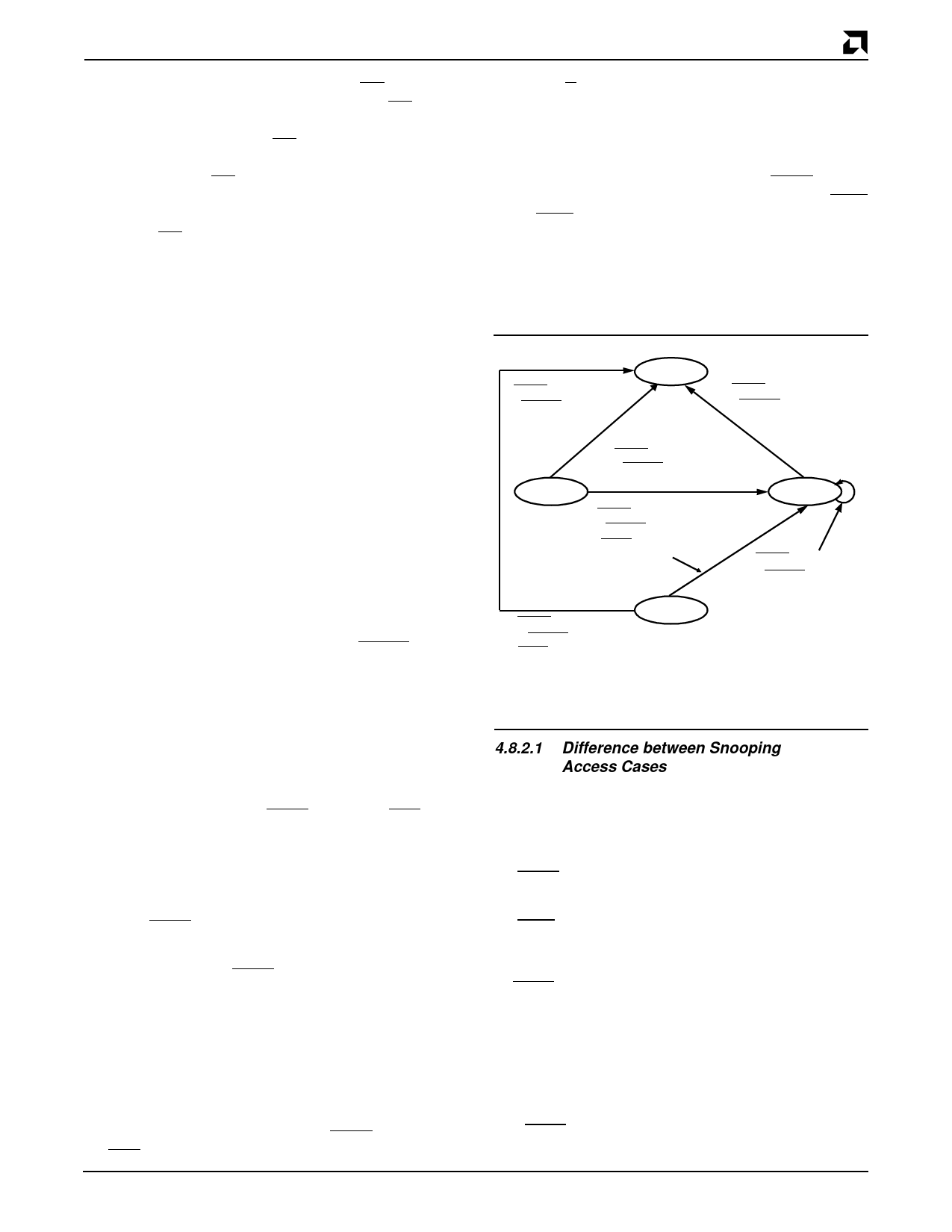
Figure 2 shows a diagram of the state transitions in-
duced by snooping accesses.
(EADS = 0 * INV = 1)
+ FLUSH = 0
Invalid
(EADS = 0 * INV = 1)
+ FLUSH = 0
EADS = 0 * INV = 0
* FLUSH = 1
Exclusive
EADS = 0 * INV = 0
* FLUSH = 1
(HITM asserted
+ write-back)
Shared
EADS = 0 * INV = 0
* FLUSH = 1
EADS = 0 * INV = 1
+ FLUSH = 0
(HITM asserted
+ write-back)
Modified
Figure 2. Snooping State Transitions
4.8.2.1 Difference between Snooping
Access Cases
Snooping accesses are external accesses to the micro-
processor. As described earlier, the snooping logic has
a set of signals independent from the processor-related
signals. Those signals are:
s EADS
s INV
s HITM
In addition to these signals, the address bus is required
as an input. This is achieved by setting AHOLD, HOLD,
or BOFF active.
Snooping can occur in parallel with a processor-initiated
access that has already been started. The two accesses
depend on each other only when a modified line is writ-
ten back. In this case, the snoop requires the use of the
cycle control signals and the data bus. The following
sections describe the scenarios for the HOLD, AHOLD,
and BOFF implementations.
Am5X86 Microprocessor
21
Share Link: 