AM29LV010B Просмотр технического описания (PDF) - Advanced Micro Devices
Номер в каталоге
Компоненты Описание
производитель
AM29LV010B
Advanced Micro Devices

AM29LV010B Datasheet PDF : 36 Pages
| |||
DATA SHEET
DEVICE BUS OPERATIONS
This section describes the requirements and use of the
device bus operations, which are initiated through the
internal command register. The command register
itself does not occupy any addressable memory loca-
tion. The register is composed of latches that store the
commands, along with the address and data informa-
tion needed to execute the command. The contents of
the register serve as inputs to the internal state
machine. The state machine outputs dictate the func-
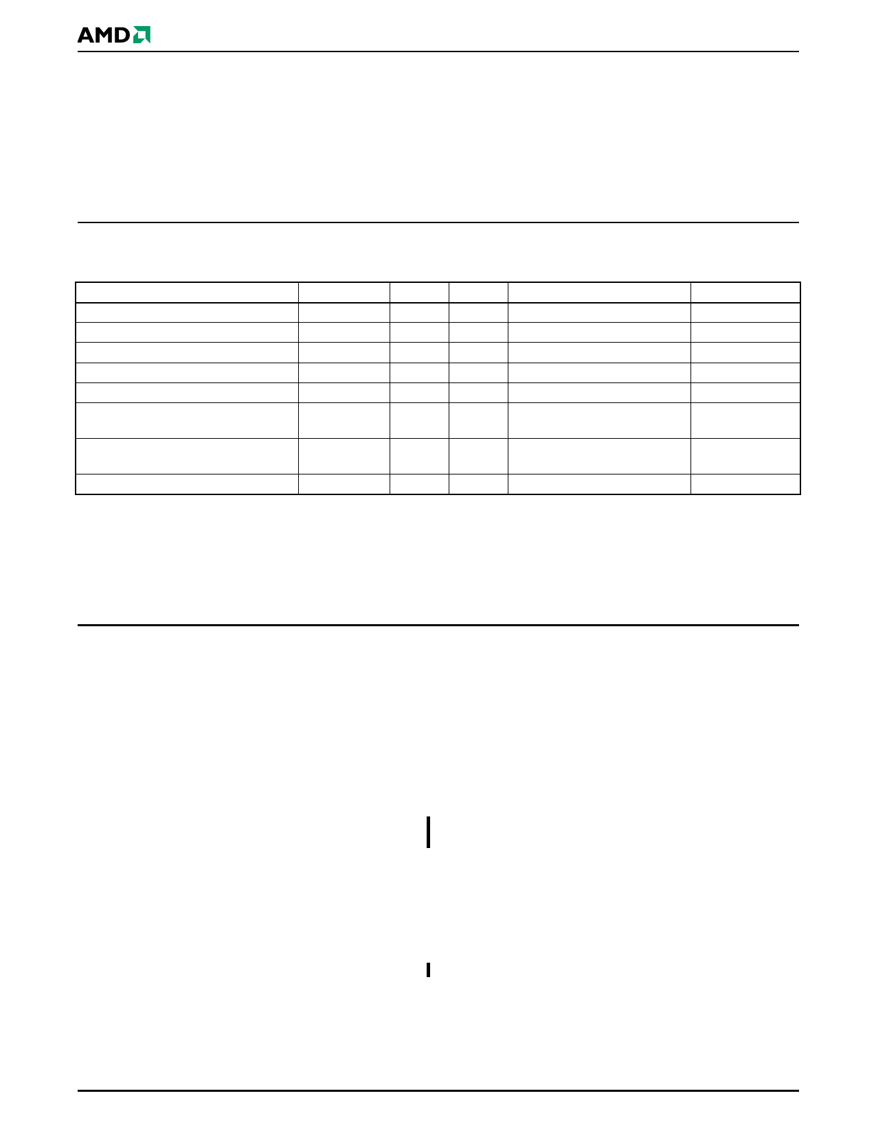
tion of the device. Table 1 lists the device bus
operations, the inputs and control levels they require,
and the resulting output. The following subsections
describe each of these operations in further detail.
Table 1. Am29LV010B Device Bus Operations
Operation
CE#
OE# WE#
Addresses (Note 1)
DQ0–DQ7
Read
Write
Standby
Output Disable
L
L
H
AIN
L
H
L
AIN
VCC ± 0.3 V
X
X
X
L
H
H
X
DOUT
DIN
High-Z
High-Z
Reset
X
X
X
X
High-Z
Sector Protect (Note 2)
L
H
L
Sector Address, A6 = L, A1 = H,
A0 = L
DIN, DOUT
Sector Unprotect (Note 2)
L
H
L
Sector Address, A6 = H, A1 =
H, A0 = L
DIN, DOUT
Temporary Sector Unprotect
X
X
X
AIN
DIN
Legend:
L = Logic Low = VIL, H = Logic High = VIH, VID = 12.0 ± 0.5 V, X = Don’t Care, AIN = Address In, DIN = Data In, DOUT = Data Out
Notes:
1. Addresses are A16–A0.
2. Sector protection/unprotection can be implemented by using programming equipment. See the “Sector Protection/Unprotec-
tion” section.
Requirements for Reading Array Data
To read array data from the outputs, the system must
drive the CE# and OE# pins to VIL. CE# is the power
control and selects the device. OE# is the output
control and gates array data to the output pins. WE#
should remain at VIH.
The internal state machine is set for reading array data
upon device power-up. This ensures that no spurious
alteration of the memory content occurs during the
power transition. No command is necessary in this
mode to obtain array data. Standard microprocessor
read cycles that assert valid addresses on the device
address inputs produce valid data on the device data
outputs. The device remains enabled for read access
until the command register contents are altered.
See “Reading Array Data” for more information. Refer
to the AC Read Operations table for timing specifica-
tions and to Figure 11 for the timing diagram. ICC1 in the
DC Characteristics table represents the active current
specification for reading array data.
Writing Commands/Command Sequences
To write a command or command sequence (which
includes programming data to the device and erasing
sectors of memory), the system must drive WE# and
CE# to VIL, and OE# to VIH.
The device features an Unlock Bypass mode to facili-
tate faster programming. Once the device enters the
Unlock Bypass mode, only two write cycles are
required to program a byte, instead of four. The “Byte
Program Command Sequence” section has details on
programming data to the device using both standard
and Unlock Bypass command sequences.
An erase operation can erase one sector, multiple sec-
tors, or the entire device. Table 2 indicates the address
space that each sector occupies. A “sector address”
consists of the address bits required to uniquely select
a sector. The “Command Definitions” section has
details on erasing a sector or the entire chip, or sus-
pending/resuming the erase operation.
After the system writes the autoselect command
sequence, the device enters the autoselect mode. The
10
Am29LV010B
22140D6 October 11, 2006
Share Link: