ALC250 Просмотр технического описания (PDF) - Unspecified
Номер в каталоге
Компоненты Описание
производитель
ALC250 Datasheet PDF : 46 Pages
| |||
ALC250 Data Sheet
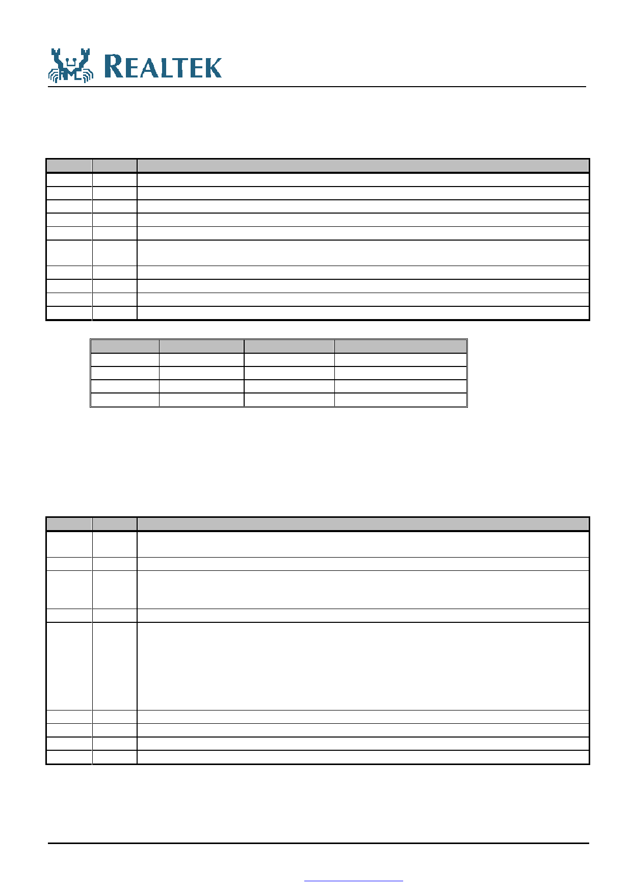
6.1.19 MX28 Extended Audio ID
Default: 0605h
The Extended Audio ID register is a read only register used to communicate information to the digital controller on two functions.
ALC250 is designed as the primary CODEC with ID is ‘00’.
Bit
15:14
13:12
11:10
9
8:6
5:4
3
2
1
0
Type
R
R
R
R/W
R
R
R
Function
ID[1:0], read as ‘00’.
Reserved, Read as 0
REV[1:0]=10 to indicate that the ALC250 is AC’97 rev2.3 compliant
AMAP read as 1 (DAC mapping based on ID)
Reserved, Read as 0
DAC Slot Assignment DSA[1:0] (Default value depends on ID[1:0])
DSA[1:0] Controls the DAC slot assignment, as described in AC’97 rev2.2.
Reserved, Read as 0
SPDIF Read as 1 (S/PDIF is supported)
DRA Read as 1
VRA Read as 1 (Variable Rate Audio is supported)
The ALC250 maps DAC slot according to the following table: (default maps to AC’97 spec. rev2.3)
DSA[1:0]
0,0
0,1
1,0
1,1
Left DAC slot #
3
7
6
10
Right DAC slot #
Comment
4
Default when ID[1:0]=00
8
Default when ID[1:0]=01,10
9
Default when ID[1:0]=11
11
-
6.1.20 MX2A Extended Audio Status and Control
Default: 0000h
This register contains two active bits for powerdown and status of the surrounding DACs. Bits 0, 1 & 2 are read/write bits which
are used to enable or disable VRA, DRA and SPDIF respectively. Bits 4 & 5 are read/write bits used to determine the AC-LINK
slot assignment of the S/PDIF. Bit 10 is a read only bit which tells the controller if the S/PDIF configuration is valid.
Bit Type
Function
15
14:11
10
9:6
5:4
3
2
1
0
R/W Validity Configuration of S/PDIF Output (VCFG)
Combines with MX3A.15 to decide validity control in S/PDIF output signal.
NA Reserved
R S/PDIF Configuration Valid (SPCV)
0: Current S/PDIF configuration {SPSA,SPSR,DAC/slot rate} is not valid.
1: Current S/PDIF configuration {SPSA,SPSR,DAC/slot rate} is valid.
Reserved
R/W SPSA[1:0], S/PDIF Slot Assignment when DRS=0
00: S/PDIF source data assigned to AC-LINK slot3/4
01: S/PDIF source data assigned to AC-LINK slot7/8 (Default when ID=00)
10: S/PDIF source data assigned to AC-LINK slot6/9 (Default when ID=01,10)
11: S/PDIF source data assigned to AC-LINK slot10/11 (Default when ID=11)
SPSA[1:0], S/PDIF-Out Slot Assignment when DRS=1(for 96K S/PDIF-Out)
01: S/PDIF-Out source is from AC-LINK slot3/4 + slot7/8.
Reserved
R/W SPDIF 1: Enable 0: Disable (SPDIFO is in high impedance)
R/W DRA 1: Enable 0: Disable
R/W VRA 1: Enable 0: Disable
If VRA = 0, ALC250 ADC/DAC operate at fixed 48KHz sampling rate. Otherwise, it operates with variable
sampling rate defined in MX2C and MX32. VRA also control write operation of MX2Cand MX32.
DRA can be written when (ID=00)&(DSA=00), otherwise it is always 0.
Two Channel AC’97 2.3 Audio Codec
15
Tel: +49(0)234-9351135 · Fax: +49(0)234-9351137 E-MAIL: info@cornelius-consult.de
Rev1.01
http://www.cornelius-consult.de
Share Link: 