X25401PI Просмотр технического описания (PDF) - Xicor -> Intersil
Номер в каталоге
Компоненты Описание
производитель
X25401PI Datasheet PDF : 14 Pages
| |||
X25401
PIN DESCRIPTIONS
Chip Select (CS)
The Chip Select input must be LOW to enable all read/
write operations. CS must remain LOW following a
Read or Write command until the data transfer is com-
plete. CS HIGH places the X25401 in the low power
standby mode and resets the instruction register. There-
fore, CS must be brought HIGH after the completion of
an operation in order to reset the instruction register in
preparation for the next command.
Serial Clock (SCK)
The Serial Clock input is used to clock all data into and
out of the device.
Serial Data In (SI)
SI is the serial data input.
Serial Data Out (SO)
SO is the serial data output. It is in the high impedance
state except during data output cycles in response to a
READ instruction.
AUTOSTORE Output (AS)
AS is an open drain output which, when asserted indi-
cates VCC has fallen below the AUTOSTORE thresh-
old (VASTH). AS may be wire-ORed with multiple open
drain outputs and used as an interrupt input to a micro-
controller or as an input to a low power reset circuit.
RECALL
RECALL LOW will initiate an internal transfer of data
from E2PROM to the RAM array.
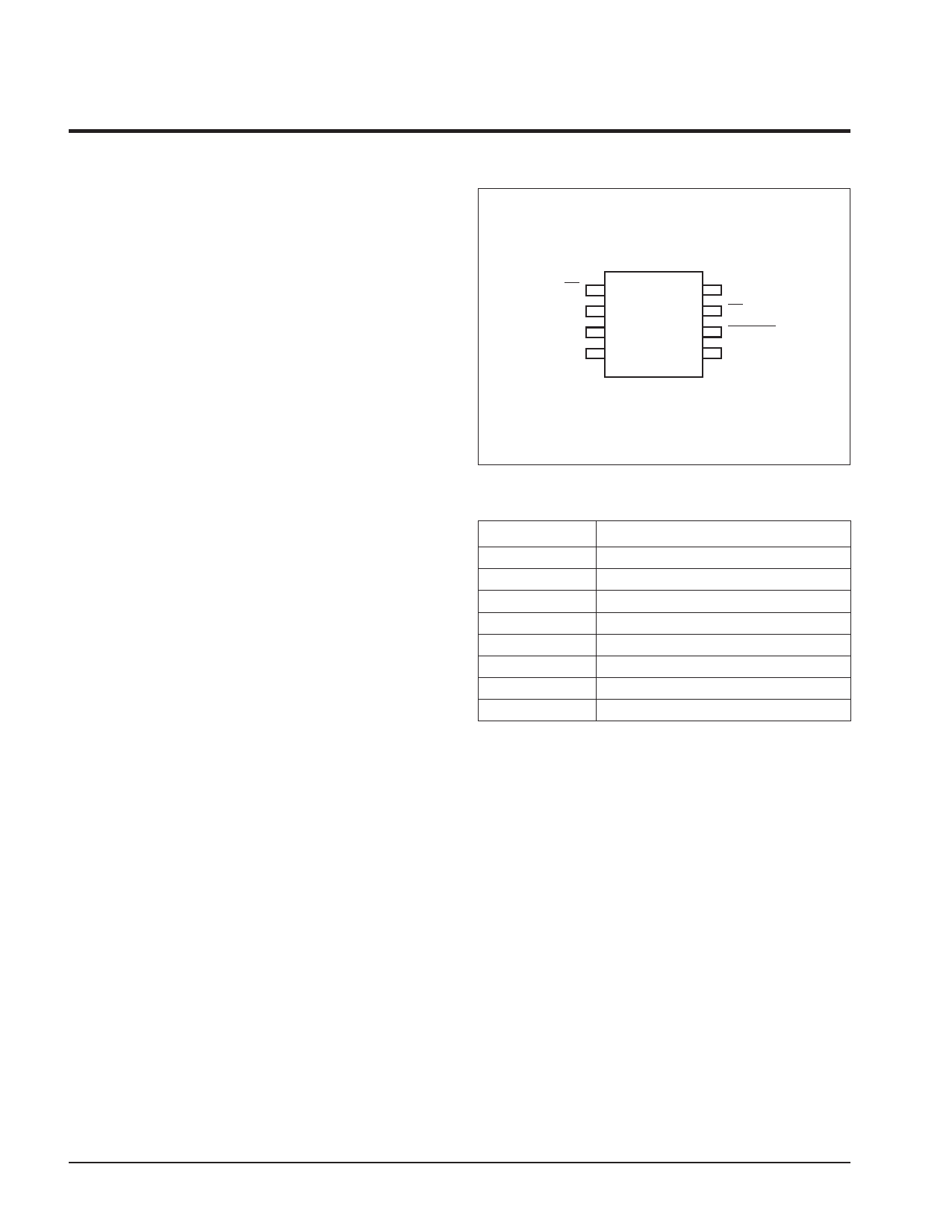
PIN CONFIGURATION
CS
SCK
SI
SO
DIP/SOIC
1
8
2
7
X25401
3
6
4
5
VCC
AS
RECALL
VSS
2051 FHD F02
PIN NAMES
Symbol
CS
SCK
SI
SO
RECALL
AS
VCC
VSS
Description
Chip Enable
Serial Clock
Serial Data In
Serial Data Out
Recall Input
AUTOSTORE Output
+5V
Ground
2051 PGM T01
2
Share Link: 