ECP050G –Я—А–Њ—Б–Љ–Њ—В—А —В–µ—Е–љ–Є—З–µ—Б–Ї–Њ–≥–Њ –Њ–њ–Є—Б–∞–љ–Є—П (PDF) - Unspecified
–Э–Њ–Љ–µ—А –≤ –Ї–∞—В–∞–ї–Њ–≥–µ
–Ъ–Њ–Љ–њ–Њ–љ–µ–љ—В—Л –Ю–њ–Є—Б–∞–љ–Є–µ
–њ—А–Њ–Є–Ј–≤–Њ–і–Є—В–µ–ї—М
ECP050G Datasheet PDF : 7 Pages
| |||
AH115 / ECP050G
¬љ Watt, High Linearity InGaP HBT Amplifier
The Communications Edge TM
Product Information
Typical Device Data
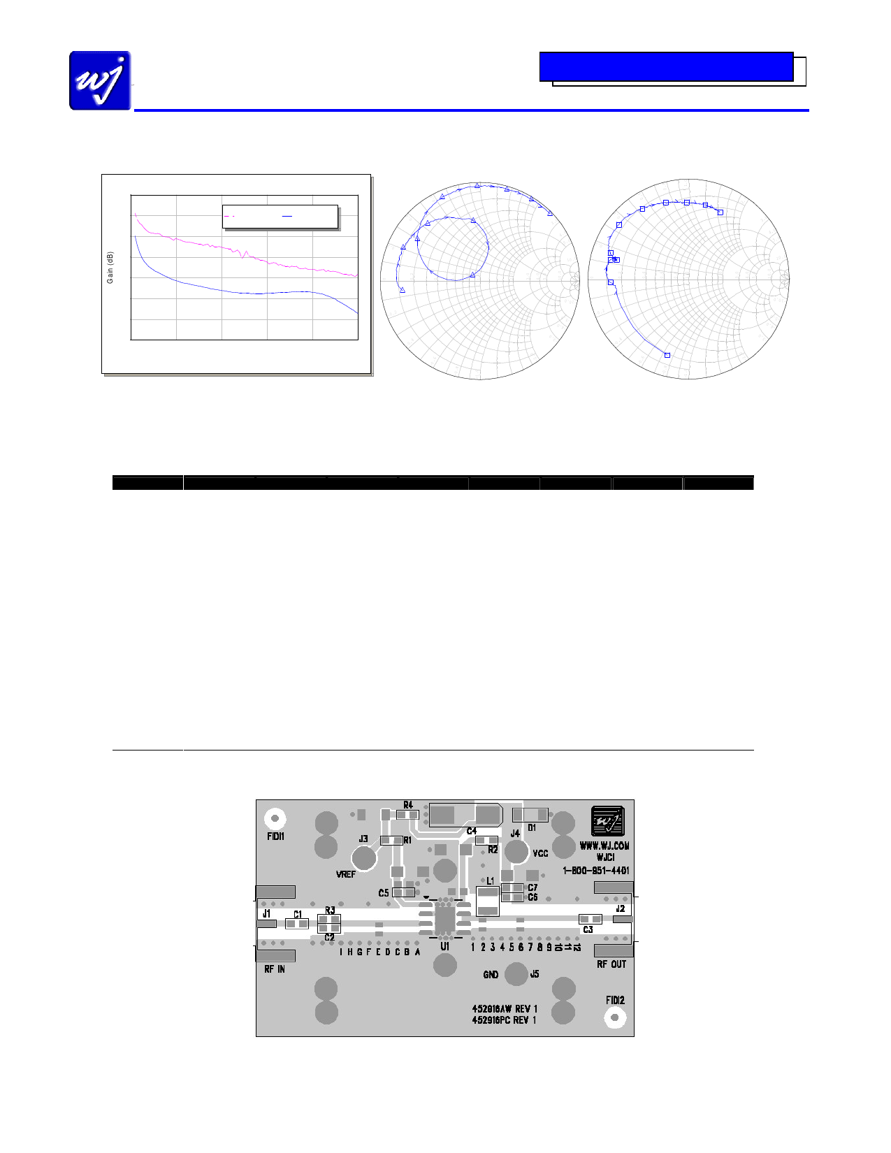
S-Parameters (Vcc = +5 V, Icc = 250 mA, T = 25¬° C, unmatched 50 ohm system)
Gain and Maximum Stable Gain
35
S11
Swp Max
5.05GHz
S22
Sw p Max
5.05GHz
30
DB(GMax)
DB(|S[2,1]|)
25
20
15
3.0
4.0
5.0
10.0
3.0
4.0
5.0
10.0
10
5
-0.2
-0.2
0
-0.4
0
0.5
1
1.5
2
2.5
Frequency (GHz)
-0.4
Swp Min
0.05GHz
Sw p Min
0.05GHz
Notes:
The gain for the unmatched device in 50 ohm system is shown as the trace in black color. For a tuned circuit for a particular frequency,
it is expected that actual gain will be higher, up to the maximum stable gain. The maximum stable gain is shown in the dashed red line.
The return loss plots are shown from 50 вАУ 5050 MHz, with markers placed at 0.5 вАУ 5.05 GHz in 0.5 GHz increments.
Freq (MHz)
50
100
200
400
600
800
1000
1200
1400
1600
1800
2000
2200
2400
2600
2800
3000
S-Parameters (Vcc = +5 V, Icc = 250 mA, T = 25¬Ґ C, unmatched 50 ohm system, calibrated to device leads)
S11 (dB)
S11 (ang)
S21 (dB)
S21 (ang)
S12 (dB)
S12 (ang)
S22 (dB)
S22 (ang)
-2.11
-172.90
25.10
133.84
-36.03
31.44
-2.06
-105.55
-1.59
-178.94
21.15
126.67
-35.22
15.04
-2.73
-138.75
-1.51
173.71
17.75
124.19
-34.29
7.30
-2.80
-160.44
-1.45
163.84
15.23
111.50
-34.45
-2.16
-2.73
-174.00
-1.58
153.68
13.69
98.94
-33.58
-2.99
-1.96
-179.13
-1.78
144.31
12.77
84.57
-32.84
-12.80
-1.68
172.00
-1.96
134.21
11.94
69.70
-32.77
-18.76
-1.85
166.98
-2.46
123.44
11.36
55.57
-31.79
-30.73
-2.14
164.05
-3.30
111.21
11.17
40.93
-31.12
-45.14
-2.30
163.07
-4.70
92.57
11.39
22.80
-30.30
-61.92
-2.52
164.84
-8.15
78.58
11.64
1.64
-29.47
-83.99
-2.43
164.25
-19.01
93.29
11.51
-25.24
-29.31
-112.79
-1.84
162.38
-9.59
177.56
10.35
-55.97
-30.51
-150.45
-1.22
155.68
-4.09
159.30
7.87
-83.78
-32.59
177.62
-1.06
147.58
-1.99
141.65
4.95
-105.90
-33.96
137.14
-1.07
139.74
-1.12
127.57
1.97
-122.86
-34.68
109.27
-1.19
132.15
-0.72
116.11
-0.88
-136.93
-35.64
81.83
-1.44
125.05
Application Circuit PC Board Layout
Circuit Board Material: .014вАЭ Getek, 4 - layer, 1 oz copper, Microstrip line details: width = .026вАЭ, spacing = .026вАЭ
The silk screen markers вАШAвАЩ, вАШBвАЩ, вАШCвАЩ, etc. and вАШ1вАЩ, вАШ2вАЩ, вАШ3вАЩ, etc. are used as placemarkers for the input and output tuning
shunt capacitors вАУ C8 and C9. The markers and vias are spaced in .050вАЭ increments.
Specifications and information are subject to change without notice
WJ Communications, Inc Phone 1-800-WJ1-4401 FAX: 408-577-6621 e-mail: sales@wj.com Web site: www.wj.com
Page 2 of 7 May 2005
Share Link: 