ADXL375 –Я—А–Њ—Б–Љ–Њ—В—А —В–µ—Е–љ–Є—З–µ—Б–Ї–Њ–≥–Њ –Њ–њ–Є—Б–∞–љ–Є—П (PDF) - Analog Devices
–Э–Њ–Љ–µ—А –≤ –Ї–∞—В–∞–ї–Њ–≥–µ
–Ъ–Њ–Љ–њ–Њ–љ–µ–љ—В—Л –Ю–њ–Є—Б–∞–љ–Є–µ
–њ—А–Њ–Є–Ј–≤–Њ–і–Є—В–µ–ї—М
ADXL375 Datasheet PDF : 32 Pages
| |||
ADXL375
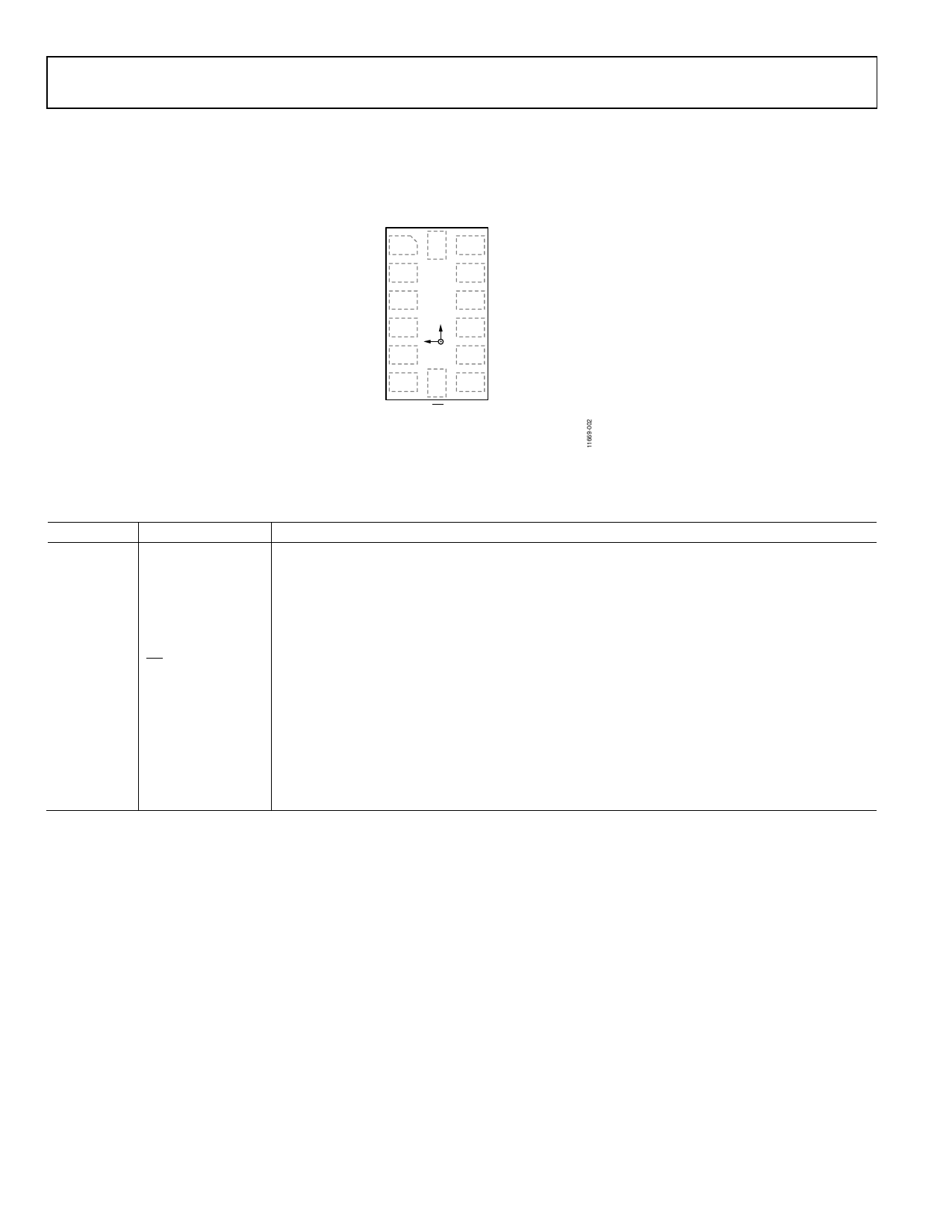
PIN CONFIGURATION AND FUNCTION DESCRIPTIONS
ADXL375
TOP VIEW
(Not to Scale)
SCL/SCLK
VDD I/O 1
14
13 SDA/SDI/SDIO
GND 2
12 SDO/ALT ADDRESS
RESERVED
GND
GND
3
11
+X
4 +Y
10
+Z
5
9
RESERVED
NC
INT2
VS
6
7
8 INT1
CS
NOTES
1. NC = NOT INTERNALLY CONNECTED.
Figure 3. Pin Configuration
Data Sheet
Table 5. Pin Function Descriptions
Pin No.
Mnemonic
Description
1
VDD I/O
Digital Interface Supply Voltage.
2
GND
Ground. This pin must be connected to ground.
3
RESERVED
Reserved. This pin must be connected to VS or left open.
4
GND
Ground. This pin must be connected to ground.
5
GND
Ground. This pin must be connected to ground.
6
VS
Supply Voltage.
7
CS
Chip Select.
8
INT1
Interrupt 1 Output.
9
INT2
Interrupt 2 Output.
10
NC
Not Internally Connected.
11
RESERVED
Reserved. This pin must be connected to ground or left open.
12
SDO/ALT ADDRESS SPI 4-Wire Serial Data Output (SDO)/I2C Alternate Address Select (ALT ADDRESS).
13
SDA/SDI/SDIO
I2C Serial Data (SDA)/SPI 4-Wire Serial Data Input (SDI)/SPI 3-Wire Serial Data Input and Output (SDIO).
14
SCL/SCLK
I2C Serial Communications Clock (SCL)/SPI Serial Communications Clock (SCLK).
Rev. 0 | Page 6 of 32
Share Link: 