ADXL375 –ü—Ä–æ—Å–º–æ—Ç—Ä —Ç–µ—Ö–Ω–∏—á–µ—Å–∫–æ–≥–æ –æ–ø–∏—Å–∞–Ω–∏—è (PDF) - Analog Devices
–ù–æ–º–µ—Ä –≤ –∫–∞—Ç–∞–ª–æ–≥–µ
–ö–æ–º–ø–æ–Ω–µ–Ω—Ç—ã –û–ø–∏—Å–∞–Ω–∏–µ
–ø—Ä–æ–∏–∑–≤–æ–¥–∏—Ç–µ–ª—å
ADXL375 Datasheet PDF : 32 Pages
| |||
ADXL375
Data Sheet
THEORY OF OPERATION
The ADXL375 is a complete 3-axis acceleration measurement
system with a measurement range of ±200 g. It measures both
dynamic acceleration resulting from motion or shock and static
acceleration, such as gravity.
The sensor is a polysilicon surface-micromachined structure
built on top of a silicon wafer. Polysilicon springs suspend the
structure over the surface of the wafer and provide resistance
against forces due to applied acceleration.
Deflection of the structure is measured using differential capac-
itors that consist of independent fixed plates and plates attached
to the moving mass. Acceleration deflects the proof mass and
unbalances the differential capacitor, resulting in a sensor output
whose amplitude is proportional to acceleration. Phase sensitive
demodulation is used to determine the magnitude and polarity
of the acceleration.
POWER SEQUENCING
Power can be applied to VS or VDD I/O in any sequence without
damaging the ADXL375. Table 7 provides a description of all
the power modes. The interface voltage level is set using the
interface supply voltage, VDD I/O, which must be present to ensure
that the ADXL375 does not create a conflict on the communi-
cation bus. For single-supply operation, VDD I/O can be the same
as the main supply, VS. In a dual-supply application, however,
VDD I/O can differ from VS to accommodate the desired interface
voltage, as long as VS is greater than or equal to VDD I/O.
After VS is applied, the device enters standby mode. In standby
mode, power consumption is minimized; the device waits for
VDD I/O to be applied and for the command to enter measurement
mode. This command can be initiated by setting the measure bit
(Bit D3) in the POWER_CTL register (Address 0x2D).
When the device is in standby mode, any register can be written
to or read from. It is recommended that the device be configured
in standby mode before enabling measurement mode. Clearing
the measure bit returns the device to standby mode.
CURRENT CONSUMPTION AND OUTPUT DATA RATE
The ADXL375 automatically modulates its current consumption
in proportion to its output data rate (see Table 6). The device
bandwidth and output data rate are specified using the rate bits
(Bits[D3:D0]) in the BW_RATE register (Address 0x2C).
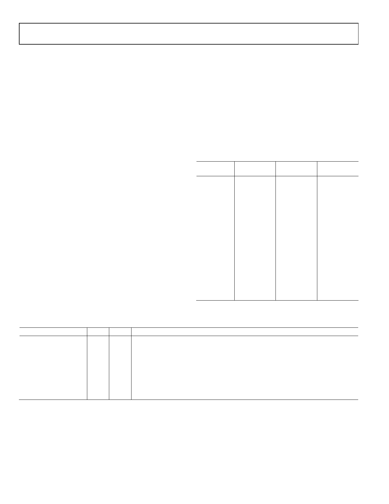
Table 6. Typical Current Consumption vs. Data Rate
(TA = 25°C, VS = 2.5 V, VDD I/O = 1.8 V)
Rate Bits
Output Data Bandwidth
Rate (Hz)
(Hz)
IDD (µA)
1111
3200
1600
145
1110
1600
800
90
1101
800
400
140
1100
400
200
140
1011
200
100
140
1010
100
50
140
1001
50
25
90
1000
25
12.5
60
0111
12.5
6.25
50
0110
6.25
3.13
40
0101
3.13
1.56
35
0100
1.56
0.78
35
0011
0.78
0.39
35
0010
0.39
0.20
35
0001
0.20
0.10
35
0000
0.10
0.05
35
Table 7. Power Modes
Power Mode
VS
Power Off
Off
Bus Disabled
On
Bus Enabled
Off
Standby or Measurement On
VDD I/O
Off
Off
On
On
Description
The device is completely off, but it is still possible for the device to create a conflict on the
communication bus.
The device is on in standby mode, but communication is unavailable and the device can create
a conflict on the communication bus. Minimize the duration of the bus disabled state during
power-up to prevent a conflict on the communication bus.
No functions are available, but the device does not create a conflict on the communication bus.
At power-up, the device is in standby mode, awaiting a command to enter measurement
mode, and all sensor functions are off. After the device is instructed to enter measurement
mode, all sensor functions are available.
Rev. 0 | Page 10 of 32
Share Link: 