ADV7177KS Просмотр технического описания (PDF) - Analog Devices
Номер в каталоге
Компоненты Описание
производитель
ADV7177KS Datasheet PDF : 38 Pages
| |||
ADV7177/ADV7178
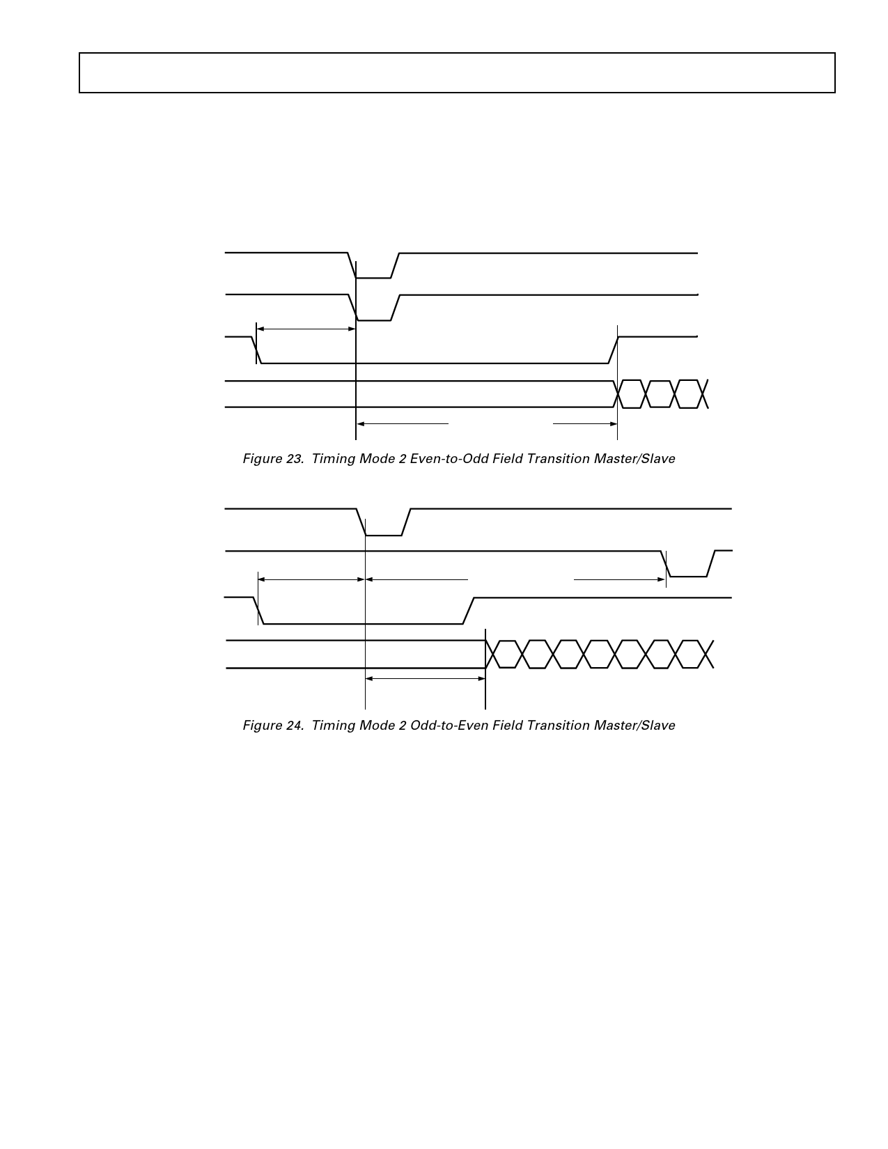
Mode 2: Master Option HSYNC, VSYNC, BLANK
(Timing Register 0 TR0 = X X X X X 1 0 1)
In this mode, the ADV7177/ADV7178 can generate horizontal and vertical SYNC signals. A coincident low transition of both
HSYNC and VSYNC inputs indicates the start of an Odd Field. A VSYNC low transition when HSYNC is high indicates the start
of an even field. The BLANK signal is optional. When the BLANK input is disabled, the ADV7177/ADV7178 automatically blanks
all normally blank lines as per CCIR-624. Mode 2 is illustrated in Figure 21 (NTSC) and Figure 22 (PAL). Figure 23 illus-
trates the HSYNC, BLANK and VSYNC for an even-to-odd field transition relative to the pixel data. Figure 24 illustrates the
HSYNC, BLANK and VSYNC for an odd-to-even field transition relative to the pixel data.
HSYNC
VSYNC
BLANK
PAL = 12 * CLOCK/2
NTSC = 16 * CLOCK/2
PIXEL
DATA
PAL = 132 * CLOCK/2
NTSC = 122 * CLOCK/2
Cb Y Cr
Figure 23. Timing Mode 2 Even-to-Odd Field Transition Master/Slave
HSYNC
VSYNC
BLANK
PAL = 12 * CLOCK/2
NTSC = 16 * CLOCK/2
PAL = 864 * CLOCK/2
NTSC = 858 * CLOCK/2
PIXEL
DATA
Cb Y
Cr
Y
Cb
PAL = 132 * CLOCK/2
NTSC = 122 * CLOCK/2
Figure 24. Timing Mode 2 Odd-to-Even Field Transition Master/Slave
REV. 0
–19–
Share Link: 