ADUM3190 Просмотр технического описания (PDF) - Analog Devices
Номер в каталоге
Компоненты Описание
производитель
ADUM3190 Datasheet PDF : 16 Pages
| |||
ADuM3190
Data Sheet
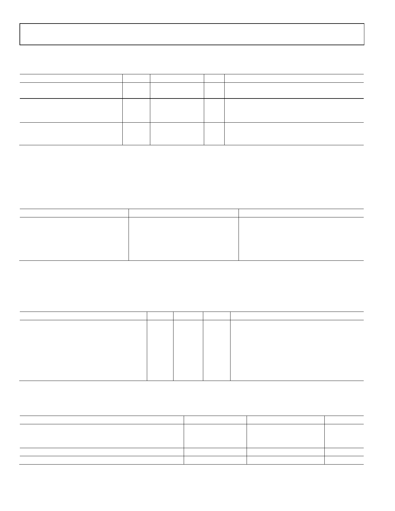
PACKAGE CHARACTERISTICS
Table 2.
Parameter
RESISTANCE
Input-to-Output1
CAPACITANCE
Input-to-Output1
Input Capacitance2
IC JUNCTION-TO-AMBIENT THERMAL
RESISTANCE
16-Lead QSOP
Symbol Min Typ Max Unit Test Conditions/Comments
RI-O
1013
Ω
CI-O
2.2
pF f = 1 MHz
CI
4.0
pF
Thermocouple located at center of package underside
θJA
76
°C/W
1 The device is considered a 2-terminal device; Pin 1 through Pin 8 are shorted together, and Pin 9 through Pin 16 are shorted together.
2 Input capacitance is from any input data pin to ground.
REGULATORY INFORMATION
The ADuM3190 is pending approval by the organizations listed in Table 3. See Table 8 and the Insulation Lifetime section for
recommended maximum working voltages for specific cross-isolation waveforms and insulation levels.
Table 3.
UL (Pending)
Recognized Under 1577 Component
Recognition Program1
Single Protection, 2500 V rms Isolation
Voltage, 16-Lead QSOP
File E214400
CSA (Pending)
Approved under CSA Component
Acceptance Notice #5A
Basic insulation per CSA 60950-1-03 and
IEC 60950-1, 400 V rms (565 V peak)
maximum working voltage
File 205078
VDE (Pending)
Certified according to DIN V VDE V 0884-10
(VDE V 0884-10): 2006-122
Reinforced insulation, 560 V peak
File 2471900-4880-0001
1 In accordance with UL 1577, each ADuM3190 is proof tested by applying an insulation test voltage ≥ 3000 V rms for 1 sec (current leakage detection limit = 5 µA).
2 In accordance with DIN V VDE V 0884-10, each ADuM3190 is proof tested by applying an insulation test voltage ≥ 1050 V peak for 1 sec (partial discharge detection
limit = 5 pC). The asterisk (*) marked on the component designates DIN V VDE V 0884-10 approval.
INSULATION AND SAFETY RELATED SPECIFICATIONS
Table 4.
Parameter
Rated Dielectric Insulation Voltage
Minimum External Air Gap (Clearance)
Symbol Value
2500
L(I01) 3.8 min
Unit
V rms
mm
Minimum External Tracking (Creepage)
L(I02) 3.1 min mm
Minimum Internal Gap (Internal Clearance)
Tracking Resistance (Comparative Tracking Index) CTI
Isolation Group
0.017 min mm
>400
V
II
Test Conditions/Comments
1-minute duration
Measured from input terminals to output terminals,
shortest distance through air
Measured from input terminals to output terminals,
shortest distance path along body
Insulation distance through insulation
DIN IEC 112/VDE 0303, Part 1
Material Group DIN VDE 0110, 1/89, Table 1
RECOMMENDED OPERATING CONDITIONS
Table 5.
Parameter
OPERATING TEMPERATURE BY MODEL
ADuM3190A/ADuM3190B
ADuM3190S/ADuM3190T
SUPPLY VOLTAGES1
INPUT SIGNAL RISE AND FALL TIMES
1 All voltages are relative to their respective grounds.
Symbol
TA
VDD1, VDD2
tR, tF
Rev. 0 | Page 4 of 16
Min
Max
Unit
−40
+85
°C
−40
+125
°C
3.0
20
V
1.0
ms
Share Link: 