ADSP-21992BST Просмотр технического описания (PDF) - Analog Devices
Номер в каталоге
Компоненты Описание
производитель
ADSP-21992BST Datasheet PDF : 60 Pages
| |||
The two address buses (PMA and DMA) share a single external
address bus, allowing memory to be expanded off-chip, and the
two data buses (PMD and DMD) share a single external data
bus. Boot memory space and I/O memory space also share the
external buses.
Program memory can store both instructions and data, permit-
ting the ADSP-21992 to fetch two operands in a single cycle, one
from program memory and one from data memory. The DSP
dual memory buses also let the embedded SHARC core fetch an
operand from data memory and the next instruction from pro-
gram memory in a single cycle.
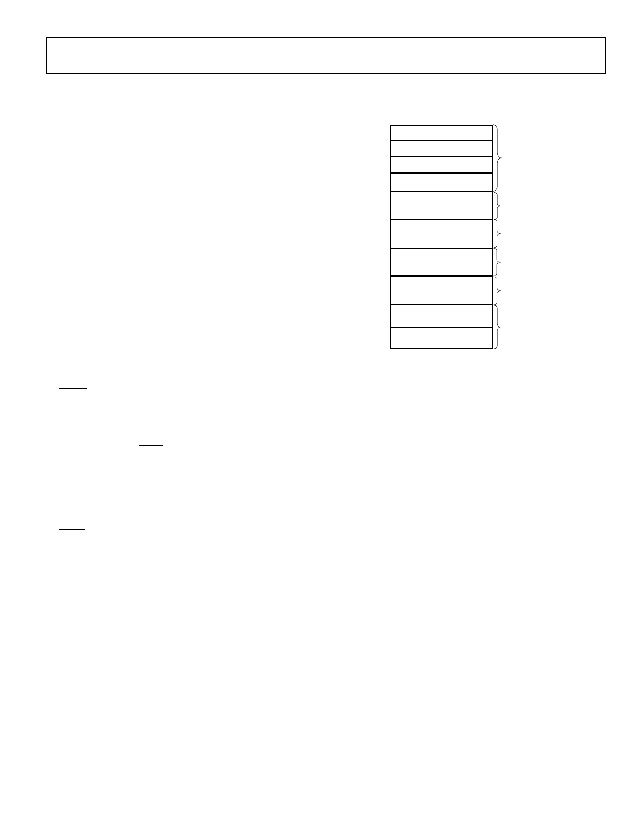
MEMORY ARCHITECTURE
The ADSP-21992 provides 48K words of on-chip SRAM mem-
ory. This memory is divided into three blocks: two 16K × 24-bit
blocks (Blocks 0 and 1) and one 16K × 16-bit block (Block 2). In
addition, the ADSP-21992 provides a 4K × 24-bit block of pro-
gram memory boot ROM (that is reserved by ADI for boot load
routines). The memory map of the ADSP-21992 is illustrated in
Figure 2.
As shown in Figure 2, the three internal memory RAM blocks
reside in memory page 0. The entire DSP memory map consists
of 256 pages (Pages 0 to 255), and each page is 64K words long.
External memory space consists of four memory banks
(Banks3–0) and supports a wide variety of memory devices.
Each bank is selectable using unique memory select lines
(MS3–0) and has configurable page boundaries, wait states, and
wait state modes. The 4K words of on-chip boot ROM populates
the top of Page 255, while the remaining 254 pages are address-
able off-chip. I/O memory pages differ from external memory in
that they are 1K word long, and the external I/O pages have
their own select pin (IOMS). Pages 31–0 of I/O memory space
reside on-chip and contain the configuration registers for the
peripherals. Both the ADSP-2199x core and DMA capable
peripherals can access the entire memory map of the DSP.
NOTE: The physical external memory addresses are limited by
20 address lines, and are determined by the external data width
and packing of the external memory space. The Strobe signals
(MS3-0) can be programmed to allow the user to change start-
ing page addresses at runtime.
ADSP-21992
0x00 0000
0x00 3FFF BLOCK 0: 16K ؋ 24-BIT PM RAM
0x00 4000
0x00 7FFF BLOCK 1: 16K ؋ 24-BIT PM RAM
0x00 8000
BLOCK 2: 16K ؋ 16-BIT DM RAM
0x00 BFFF
0x00 C000
RESERVED (16K)
0x00 FFFF
0x01 0000
EXTERNAL MEMORY
(4M–64K)
0x40 0000
EXTERNAL MEMORY (4M)
0x80 0000
EXTERNAL MEMORY (4M)
0xC0 0000
0xFF 0000
0xFF 0FFF
0xFF 1000
0xFF FFFF
EXTERNAL MEMORY
(4M–64K)
BLOCK 3: 4K ؋ 24-BIT
PM ROM
UNUSED ON-CHIP
MEMORY (60K)
PAGE 0 (64K) ON-CHIP
(0 WAIT STATE)
PAGES 1 TO 63 BANK 0
(OFF-CHIP) MS0
PAGES 64 TO 127 BANK 1
(OFF-CHIP) MS1
PAGES 128 TO 191 BANK 2
(OFF-CHIP) MS2
PAGES 192 TO 254 BANK 3
(OFF-CHIP) MS3
PAGE 255
(INCLUDES ON-CHIP BOOT ROM)
Figure 3. Core Memory Map at Reset
Internal (On-Chip) Memory
The unified program and data memory space of the
ADSP-21992 consists of 16M locations that are accessible
through two 24-bit address buses, the PMA, and DMA buses.
The DSP uses slightly different mechanisms to generate a 24-bit
address for each bus. The DSP has three functions that support
access to the full memory map.
• The DAGs generate 24-bit addresses for data fetches from
the entire DSP memory address range. Because DAG index
(address) registers are 16 bits wide and hold the lower
16 bits of the address, each of the DAGs has its own 8-bit
page register (DMPGx) to hold the most significant eight
address bits. Before a DAG generates an address, the pro-
gram must set the DAG DMPGx register to the appropriate
memory page. The DMPG1 register is also used as a page
register when accessing external memory. The program
must set DMPG1 accordingly, when accessing data vari-
ables in external memory. A “C” program macro is
provided for setting this register.
• The program sequencer generates the addresses for
instruction fetches. For relative addressing instructions, the
program sequencer bases addresses for relative jumps, calls,
and loops on the 24-bit program counter (PC). In direct
addressing instructions (two word instructions), the
instruction provides an immediate 24-bit address value.
The PC allows linear addressing of the full 24-bit
address range.
• For indirect jumps and calls that use a 16-bit DAG address
register for part of the branch address, the program
sequencer relies on an 8-bit indirect jump page (IJPG)
Rev. A | Page 5 of 60 | August 2007
Share Link: 