ADSP-21991BST Просмотр технического описания (PDF) - Analog Devices
Номер в каталоге
Компоненты Описание
производитель
ADSP-21991BST Datasheet PDF : 44 Pages
| |||
ADSP-21991
255) are available for external peripheral devices. External I/O
pages have their own select pin (IOMS). The DSP instruction
set provides instructions for accessing I/O space.
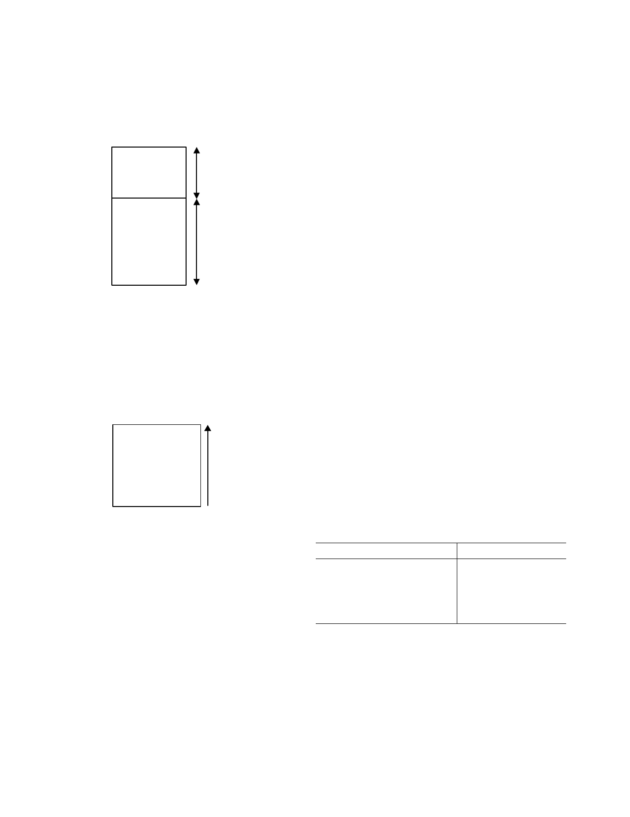
0x00::0x000
0x1F::0x3FF
0x20::0x000
ON-CHIP
PERIPHERALS
16-BITS
OFF-CHIP
PERIPHERALS
16-BITS
PAGES 0 TO 31
1024 WORDS/PAGE
2 PERIPHERALS/PAGE
PAGES 32 TO 255
1024 WORDS/PAGE
0xFF::0x3FF
Figure 3. I/O Memory Map
Boot Memory Space
Boot memory space consists of one off-chip bank with 254 pages.
The BMS memory bank pin selects boot memory space. Both
the ADSP-219x core and DMA capable peripherals can access
the off-chip boot memory space of the DSP. After reset, the DSP
always starts executing instructions from the on-chip boot ROM.
0x01 0000
OFF-CHIP
BOOT MEMORY
16-BITS
PAGES 1 TO 254
64K WORDS/PAGE
0xFE 0000
Figure 4. Boot Memory Map
Bus Request and Bus Grant
The ADSP-21991 can relinquish control of the data and address
buses to an external device. When the external device requires
access to the bus, it asserts the bus request (BR) signal. The (BR)
signal is arbitrated with core and peripheral requests. External
Bus requests have the lowest priority. If no other internal request
is pending, the external bus request will be granted. Due to syn-
chronizer and arbitration delays, bus grants will be provided with
a minimum of three peripheral clock delays. The ADSP-21991
will respond to the bus grant by:
• Three-stating the data and address buses and the MS3–0,
BMS, IOMS, RD, and WR output drivers.
• Asserting the bus grant (BG) signal.
The ADSP-21991 will halt program execution if the bus is
granted to an external device and an instruction fetch or data
read/write request is made to external general-purpose or periph-
eral memory spaces. If an instruction requires two external
memory read accesses, the bus will not be granted between the
two accesses. If an instruction requires an external memory read
and an external memory write access, the bus may be granted
between the two accesses. The external memory interface can be
configured so that the core will have exclusive use of the interface.
DMA and Bus Requests will be granted. When the external
device releases BR, the DSP releases BG and continues program
execution from the point at which it stopped.
The bus request feature operates at all times, even while the DSP
is booting and RESET is active.
The ADSP-21991 asserts the BGH pin when it is ready to start
another external port access, but is held off because the bus was
previously granted. This mechanism can be extended to define
more complex arbitration protocols for implementing more
elaborate multimaster systems.
DMA Controller
The ADSP-21991 has a DMA controller that supports
automated data transfers with minimal overhead for the DSP
core. Cycle stealing DMA transfers can occur between the
ADSP-21991 internal memory and any of its DMA capable
peripherals. Additionally, DMA transfers can be accomplished
between any of the DMA capable peripherals and external
devices connected to the external memory interface. DMA
capable peripherals include the SPORT and SPI ports, and ADC
Control module. Each individual DMA capable peripheral has a
dedicated DMA channel. To describe each DMA sequence, the
DMA controller uses a set of parameters—called a DMA descrip-
tor. When successive DMA sequences are needed, these DMA
descriptors can be linked or chained together, so the completion
of one DMA sequence auto initiates and starts the next sequence.
DMA sequences do not contend for bus access with the DSP
core, instead DMAs “steal” cycles to access memory.
All DMA transfers use the DMA bus shown in Figure 1 on
Page 4. Because all of the peripherals use the same bus, arbitra-
tion for DMA bus access is needed. The arbitration for DMA bus
access appears in Table 1.
Table 1. I/O Bus Arbitration Priority
DMA Bus Master
SPORT Receive DMA
SPORT Transmit DMA
ADC Control DMA
SPI Receive/Transmit DMA
Memory DMA
Arbitration Priority
0—Highest
1
2
3
4—Lowest
DSP Peripherals Architecture
The ADSP-21991 contains a number of special purpose,
embedded control peripherals, which can be seen in the Func-
tional Block Diagram on Page 1. The ADSP-21991 contains a
high performance, 8-channel, 14-bit ADC system with dual
channel simultaneous sampling ability across four pairs of inputs.
An internal precision voltage reference is also available as part of
the ADC system. In addition, a 3-phase, 16-bit, center based
PWM generation unit can be used to produce high accuracy
PWM signals with minimal processor overhead. The ADSP-
21991 also contains a flexible incremental encoder interface unit
–6–
REV. 0
Share Link: 