ADSP-2184L Просмотр технического описания (PDF) - Analog Devices
Номер в каталоге
Компоненты Описание
производитель
ADSP-2184L Datasheet PDF : 48 Pages
| |||
ADSP-2184L/ADSP-2185L/ADSP-2186L/ADSP-2187L
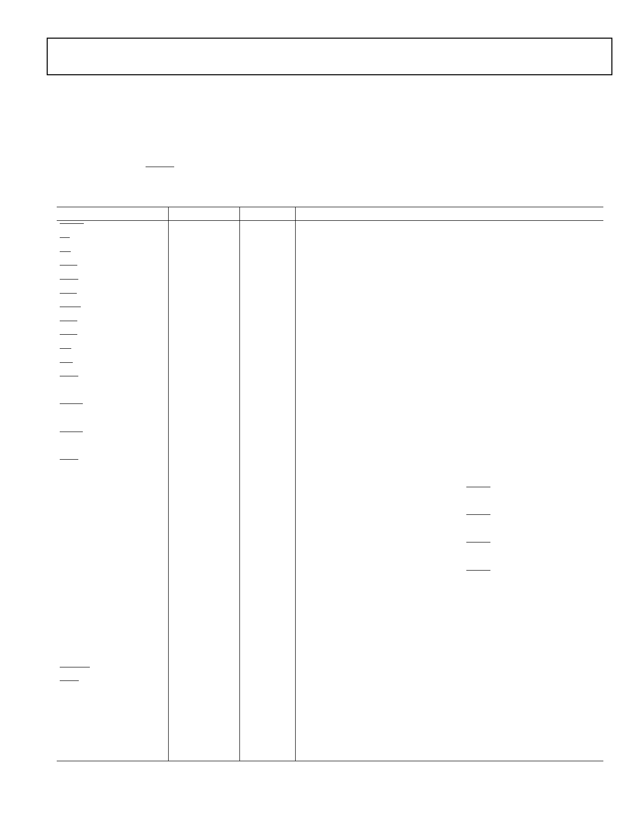
PIN DESCRIPTIONS
ADSP-218xL series members are available in a 100-lead LQFP
package and a 144-ball BGA package. In order to maintain max-
imum functionality and reduce package size and pin count,
some serial port, programmable flag, interrupt and external bus
pins have dual, multiplexed functionality. The external bus pins
are configured during RESET only, while serial port pins are
software configurable during program execution. Flag and
interrupt functionality is retained concurrently on multiplexed
pins. In cases where pin functionality is reconfigurable, the
default state is shown in plain text in Table 9, while alternate
functionality is shown in italics.
Table 9. Common-Mode Pins
Pin Name
RESET
BR
BG
BGH
DMS
PMS
IOMS
BMS
CMS
RD
WR
IRQ2/
PF7
IRQL1/
PF6
IRQL0/
PF5
IRQE/
PF4
Mode D2/
PF3
Mode C/
PF2
Mode B/
PF1
Mode A/
PF0
CLKIN
XTAL
CLKOUT
SPORT0
SPORT1/
IRQ1–0, FI, FO
PWD
PWDACK
FL0, FL1, FL2
VDDINT
VDDEXT
GND
No. of Pins
I/O
1
I
1
I
1
O
1
O
1
O
1
O
1
O
1
O
1
O
1
O
1
O
1
I
I/O
1
I
I/O
1
I
I/O
1
I
I/O
1
I
I/O
1
I
I/O
1
I
I/O
1
I
I/O
1
I
1
O
1
O
5
I/O
5
I/O
1
I
1
O
3
O
2
I
4
I
10
I
Function
Processor Reset Input
Bus Request Input
Bus Grant Output
Bus Grant Hung Output
Data Memory Select Output
Program Memory Select Output
Memory Select Output
Byte Memory Select Output
Combined Memory Select Output
Memory Read Enable Output
Memory Write Enable Output
Edge- or Level-Sensitive Interrupt Request1
Programmable I/O Pin
Level-Sensitive Interrupt Requests1
Programmable I/O Pin
Level-Sensitive Interrupt Requests1
Programmable I/O Pin
Edge-Sensitive Interrupt Requests1
Programmable I/O Pin
Mode Select Input—Checked Only During RESET
Programmable I/O Pin During Normal Operation
Mode Select Input—Checked Only During RESET
Programmable I/O Pin During Normal Operation
Mode Select Input—Checked Only During RESET
Programmable I/O Pin During Normal Operation
Mode Select Input—Checked Only During RESET
Programmable I/O Pin During Normal Operation
Clock Input
Quartz Crystal Output
Processor Clock Output
Serial Port I/O Pins
Serial Port I/O Pins
Edge- or Level-Sensitive Interrupts, FI, FO3
Power-Down Control Input
Power-Down Acknowledge Control Output
Output Flags
Internal VDD (1.8 V) Power (LQFP)
External VDD (1.8 V, 2.5 V, or 3.3 V) Power (LQFP)
Ground (LQFP)
Rev. C | Page 17 of 48 | January 2008
Share Link: 