ADSP-2184L(Rev0) Просмотр технического описания (PDF) - Analog Devices
Номер в каталоге
Компоненты Описание
производитель
ADSP-2184L Datasheet PDF : 31 Pages
| |||
ADSP-2184L
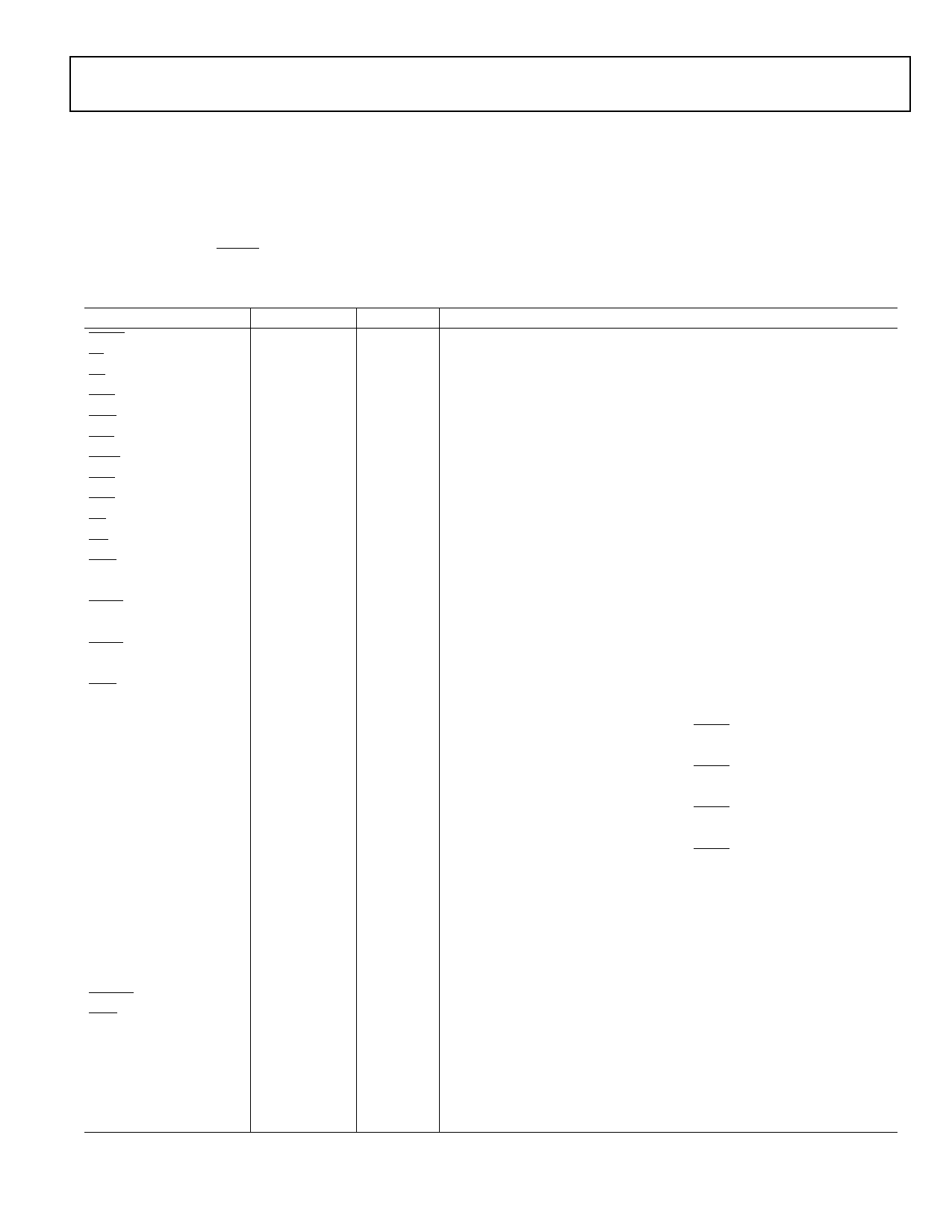
Parameter
Min
Max
Unit
Bus Request–Bus Grant
Timing Requirements:
tBH
BR Hold after CLKOUT High1
tBS
BR Setup before CLKOUT Low1
Switching Characteristics:
tSD
tSDB
tSE
tSEC
tSDBH
tSEH
CLKOUT High to xMS, RD, WR Disable
xMS, RD, WR Disable to BG Low
BG High to xMS, RD, WR Enable
xMS, RD, WR Enable to CLKOUT High
xMS, RD, WR Disable to BGH Low2
BGH High to xMS, RD, WR Enable2
0.25 tCK + 2
ns
0.25 tCK + 17
ns
0.25 tCK + 10
ns
0
ns
0
ns
0.25 tCK – 7
ns
0
ns
0
ns
NOTES
xMS = PMS, DMS, CMS, IOMS, BMS.
1BR is an asynchronous signal. If BR meets the setup/hold requirements, it will be recognized during the current clock cycle; otherwise the signal will be recognized on
the following cycle. Refer to the ADSP-2100 Family User’s Manual, Third Edition for BR/BG cycle relationships.
2BGH is asserted when the bus is granted and the processor requires control of the bus to continue.
CLKOUT
BR
CLKOUT
PMS, DMS
BMS, RD
WR
BG
BGH
tBH
tBS
tSD
tSEC
tSDB
tSE
tSDBH
tSEH
Figure 11. Bus Request–Bus Grant
REV. 0
–17–
Share Link: 