ADSP-2184L(Rev0) Просмотр технического описания (PDF) - Analog Devices
Номер в каталоге
Компоненты Описание
производитель
ADSP-2184L Datasheet PDF : 31 Pages
| |||
SPECIFICATIONS
RECOMMENDED OPERATING CONDITIONS
Parameter
Min
VDD
3.0
TAMB
–40
B Grade
Max
3.6
+85
ADSP-2184L
Unit
V
°C
ELECTRICAL CHARACTERISTICS
Parameter
VIH
VIH
VIL
VOH
VOL
IIH
IIL
IOZH
IOZL
IDD
IDD
CI
CO
Hi-Level Input Voltage1, 2
Hi-Level CLKIN Voltage
Lo-Level Input Voltage1, 3
Hi-Level Output Voltage1, 4, 5
Lo-Level Output Voltage1, 4, 5
Hi-Level Input Current3
Lo-Level Input Current3
Three-State Leakage Current7
Three-State Leakage Current7
Supply Current (Idle)9
Supply Current (Dynamic)10, 11
Input Pin Capacitance3, 6, 12
Output Pin Capacitance6, 7, 12, 13
Test Conditions
@ VDD = max
@ VDD = max
@ VDD = min
@ VDD = min
IOH = –0.5 mA
@ VDD = min
IOH = –100 µA6
@ VDD = min
IOL = 2 mA
@ VDD = max
VIN = VDD max
@ VDD = max
VIN = 0 V
@ VDD = max
VIN = VDD max8
@ VDD = max
VIN = 0 V8
@ VDD = 3.3
@ VDD = 3.3
TAMB = +25°C
tCK = 25 ns
@ VIN = 2.5 V,
fIN = 1.0 MHz,
TAMB = +25°C
@ VIN = 2.5 V,
fIN = 1.0 MHz,
TAMB = +25°C
B Grade
Min Typ
2.0
2.2
2.4
VDD – 0.3
8.6
Max
0.8
0.4
10
10
10
10
42
8
8
Unit
V
V
V
V
V
V
µA
µA
µA
µA
mA
mA
pF
pF
NOTES
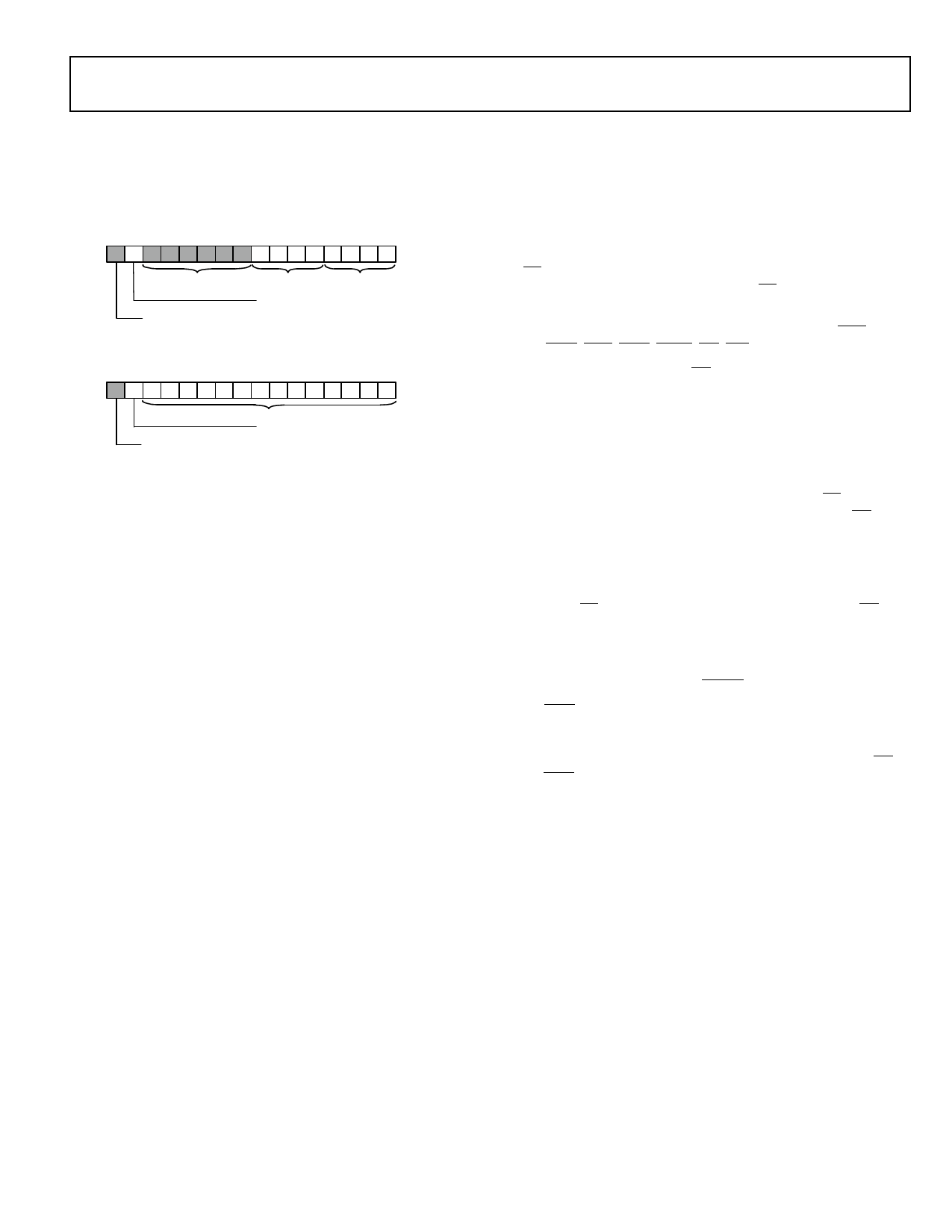
1 Bidirectional pins: D0–D23, RFS0, RFS1, SCLK0, SCLK1, TFS0, TFS1, A1–A13, PF0–PF7.
2 Input only pins: RESET, BR, DR0, DR1, PWD.
3 Input only pins: CLKIN, RESET, BR, DR0, DR1, PWD.
4 Output pins: BG, PMS, DMS, BMS, IOMS, CMS, RD, WR, PWDACK, A0, DT0, DT1, CLKOUT, FL2–0, BGH.
5 Although specified for TTL outputs, all ADSP-2184L outputs are CMOS-compatible and will drive to V DD and GND, assuming no dc loads.
6 Guaranteed but not tested.
7 Three-statable pins: A0–A13, D0–D23, PMS, DMS, BMS, IOMS, CMS, RD, WR, DT0, DT1, SCLK0, SCLK1, TFS0, TFS1, RFS0, RFS1, PF0–PF7.
8 0 V on BR.
9 Idle refers to ADSP-2184L state of operation during execution of IDLE instruction. Deasserted pins are driven to either V DD or GND.
10 IDD measurement taken with all instructions executing from internal memory. 50% of the instructions are multifunction (types 1, 4, 5, 12, 13, 14), 30% are type 2
and type 6, and 20% are idle instructions.
11 VIN = 0 V and 3 V. For typical figures for supply currents, refer to Power Dissipation section.
12Applies to LQFP package type.
13Output pin capacitance is the capacitive load for any three-stated output pin.
Specifications subject to change without notice.
REV. 0
–13–
Share Link: 