ADSP-21469KBZ-ENG Просмотр технического описания (PDF) - Analog Devices
Номер в каталоге
Компоненты Описание
производитель
ADSP-21469KBZ-ENG Datasheet PDF : 56 Pages
| |||
Preliminary Technical Data
to four separate devices to coexist, supporting any desired com-
bination of synchronous and asynchronous device types. Non
DDR2 DRAM external memory address space is shown in
Table 4.
External Memory Execution
In the ADSP-21469, the program sequencer can execute code
directly from external memory bank 0 (SRAM, as well as DDR2
DRAM). This allows more options to a user in terms of code
and data storage. With external execution, programs run at
slower speeds since 48-bit instructions are fetched in parts from
a 16-bit external bus coupled with the inherent latency of fetch-
ing instructions from DDR2 DRAM. VISA mode and SIMD
mode accesses are supported for DDR2 space. However, exter-
nal memory execution from DDR2 space is different for VISA
and non-VISA mode.
DDR2 Support
The ADSP-21469 supports a 16-bit DDR interface operating at a
maximum frequency of half the core clock. Execution from
external memory is supported. External memory up to 2 Gbits
can be supported. Delay line DMA functionality supported.
DDR2 DRAM Controller
The DDR2 DRAM controller provides an 16-bit interface to up
to four separate banks of industry-standard DDR2 DRAM
devices. Fully compliant with the DDR2 DRAM standard, each
bank can has its own memory select line (DDR2_CS3-
DDR2_CS0), and can be configured to contain between 32M
bytes and 256M bytes of memory. DDR2 DRAM external mem-
ory address space is shown in Table 5
A set of programmable timing parameters is available to config-
ure the DDR2 DRAM banks to support memory devices.
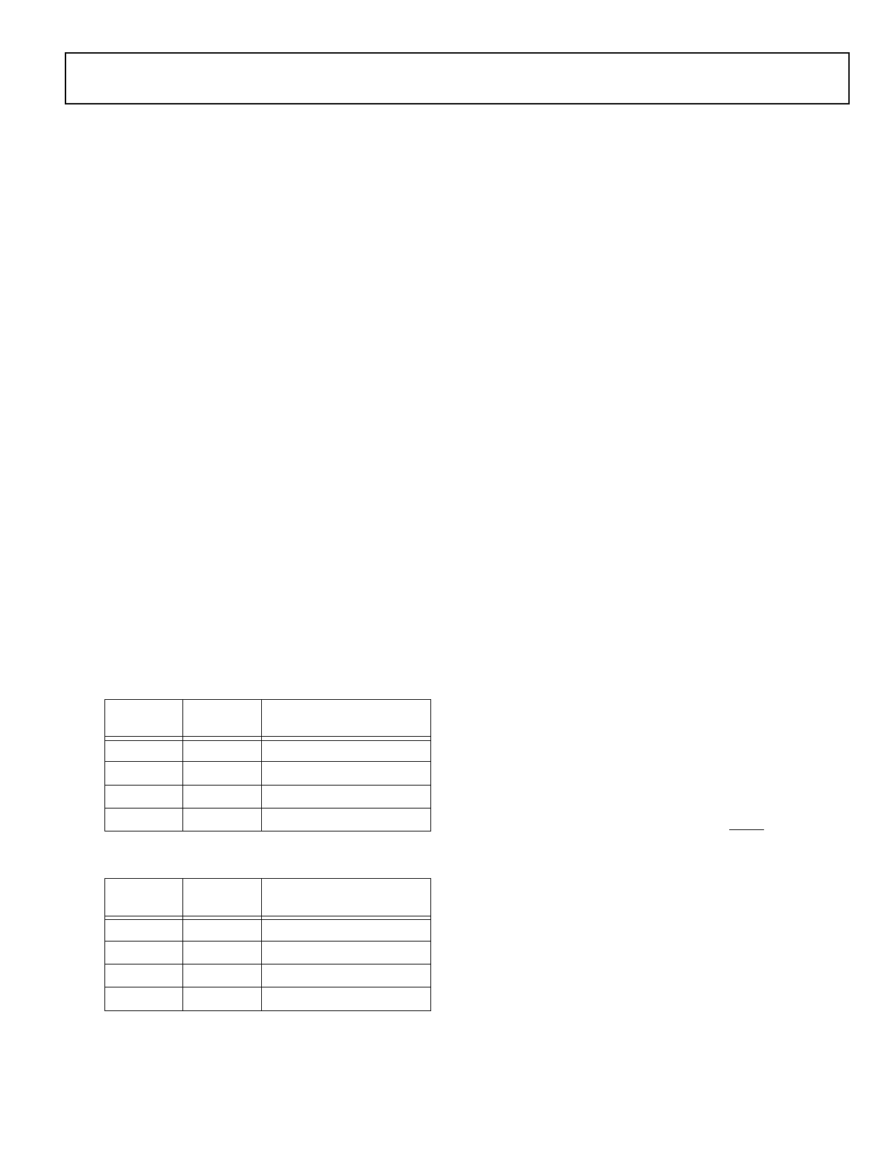
Table 4. External Memory for Non DDR2 DRAM Addresses
Bank
Bank 0
Bank 1
Bank 2
Bank 3
Size in
Words
14M
16M
16M
16M
Address Range
0x0020 0000 – 0x00FF FFFF
0x0400 0000 – 0x04FF FFFF
0x0800 0000 – 0x08FF FFFF
0x0C00 0000 – 0x0CFF FFFF
Table 5. External Memory for DDR2 DRAM Addresses
Bank
Bank 0
Bank 1
Bank 2
Bank 3
Size in
Words
62M
64M
64M
64M
Address Range
0x0020 0000 – 0x03FF FFFF
0x0400 0000 – 0x07FF FFFF
0x0800 0000 – 0x0BFF FFFF
0x0C00 0000 – 0x0FFF FFFF
ADSP-21469/ADSP-21469W
Note that the external memory bank addresses shown are for
normal-word (32-bit) accesses. If 48-bit instructions as well as
32-bit data are both placed in the same external memory bank,
care must be taken while mapping them to avoid overlap. In
case of 32-bit wide external memory, two 48-bit instructions
will be stored in three 32-bit wide memory locations. For exam-
ple, if 2k instructions are placed in 32-bit wide external memory
starting at the bank 0 normal-word base address 0x0030 0000
(corresponding to instruction address 0x0020 0000) and ending
at address 0x0030 0BFF (corresponding to instruction address
0x0020 07FF), then data buffers can be placed starting at an
address that is offset by 3k 32-bit words (for example, starting at
0x0030 0C00).
Asynchronous Memory Controller
The asynchronous memory controller provides a configurable
interface for up to four separate banks of memory or I/O
devices. Each bank can be independently programmed with dif-
ferent timing parameters, enabling connection to a wide variety
of memory devices including SRAM, flash, and EPROM, as well
as I/O devices that interface with standard memory control
lines. Bank 0 occupies a 14M word window and banks 1, 2, and
3 occupy a 16M word window in the processor’s address space
but, if not fully populated, these windows are not made contigu-
ous by the memory controller logic.
The asynchronous memory controller is capable of a maximum
throughput of TBD Mbps using a TBD MHz external bus speed.
Other features include 8 to 32-bit packing and unpacking, boot-
ing from bank select 1, and support for delay line DMA.
Shared External Memory
The ADSP-21469 processor supports connecting to common
shared external DDR2 memory with other ADSP-21469 proces-
sors to create shared external bus processor systems. This
support includes:
• Distributed, on-chip arbitration for the shared external bus
• Fixed and rotating priority bus arbitration
• Bus time-out logic
• Bus lock
Multiple processors can share the external bus with no addi-
tional arbitration logic. Arbitration logic is included on-chip to
allow the connection of up to TBD processors.
Bus arbitration is accomplished through the BR6-1 signals and
the priority scheme for bus arbitration is determined by the set-
ting of the RPBA pin. Table 6 on Page 12 provides descriptions
of the pins used in multiprocessor systems.
INPUT/OUTPUT FEATURES
The ADSP-21469 I/O processor provides 36 channels of DMA,
as well as an extensive set of peripherals. These include a 20 lead
digital applications interface, which controls:
• Eight serial ports
• S/PDIF receiver/transmitter
Rev. PrB | Page 7 of 56 | November 2008
Share Link: 