ADSP-21469KBCZ-3(Rev0) Просмотр технического описания (PDF) - Analog Devices
Номер в каталоге
Компоненты Описание
производитель
ADSP-21469KBCZ-3 Datasheet PDF : 72 Pages
| |||
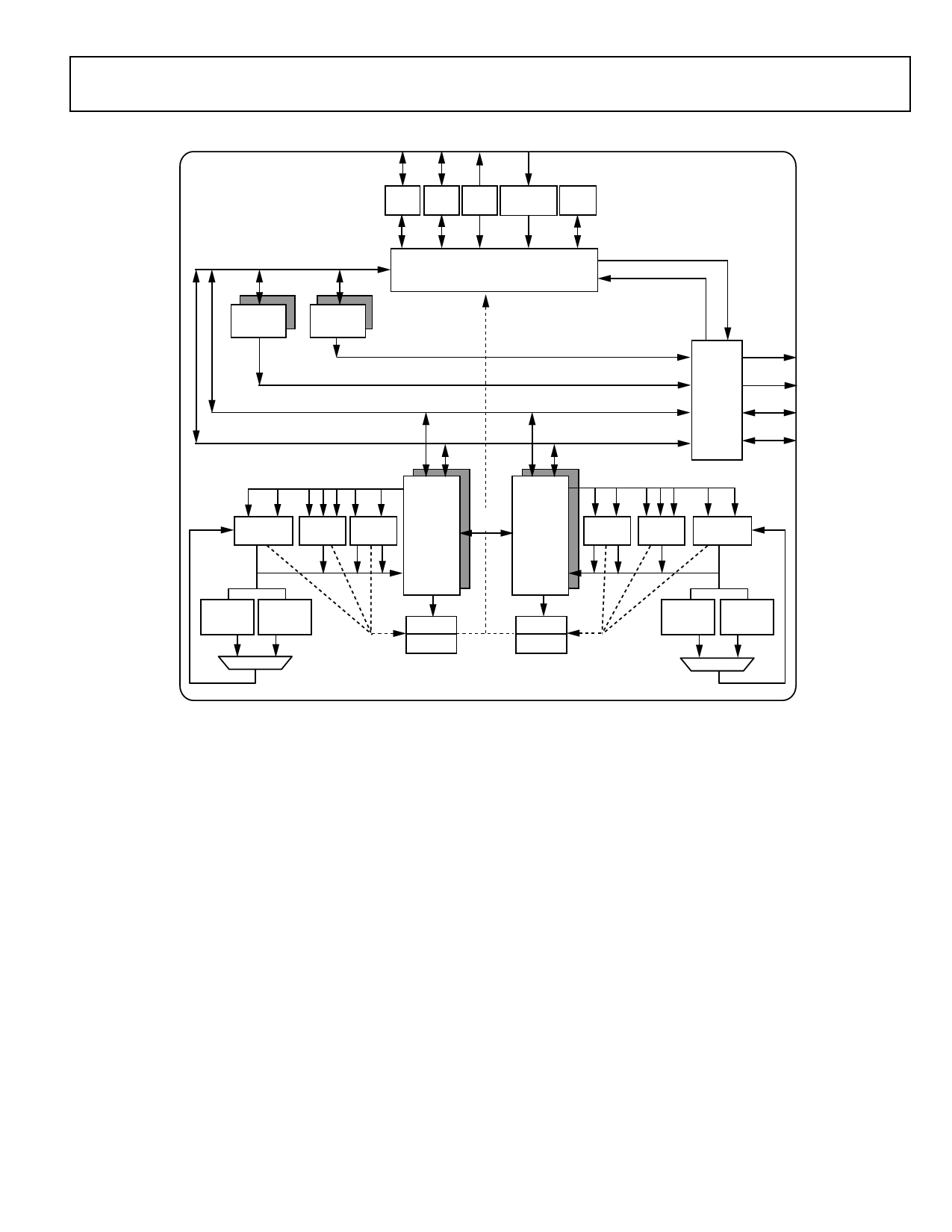
ADSP-21469
S
SIMD Core
DMD/PMD 64
DAG1
16x32
DAG2
16x32
JTAG FLAG TIMER INTERRUPT CACHE
5 STAGE
PROGRAM SEQUENCER
PM ADDRESS 24
PM DATA 48
PM ADDRESS 32
DM ADDRESS 32
PM DATA 64
DM DATA 64
SYSTEM
I/F
USTAT
4x32-BIT
PX
64-BIT
MULTIPLIER SHIFTER ALU
RF
Rx/Fx
PEx
16x40-BIT
DATA
SWAP
RF
Sx/SFx
PEy
16x40-BIT
ALU
SHIFTER MULTIPLIER
MRF
80-BIT
MRB
80-BIT
ASTATx
STYKx
ASTATy
STYKy
MSB
80-BIT
MSF
80-BIT
Figure 2. SHARC Core Block Diagram
other data structures required in digital signal processing, and
are commonly used in digital filters and Fourier transforms.
The two DAGs of the processors contain sufficient registers to
allow the creation of up to 32 circular buffers (16 primary regis-
ter sets, 16 secondary). The DAGs automatically handle address
pointer wraparound, reduce overhead, increase performance,
and simplify implementation. Circular buffers can start and end
at any memory location.
Flexible Instruction Set
The 48-bit instruction word accommodates a variety of parallel
operations for concise programming. For example, the
ADSP-21469 can conditionally execute a multiply, an add, and a
subtract in both processing elements while branching and fetch-
ing up to four 32-bit values from memory—all in a single
instruction.
Variable Instruction Set Architecture (VISA)
In addition to supporting the standard 48-bit instructions from
previous SHARC processors, the ADSP-21469 supports new
instructions of 16 and 32 bits. This feature, called Variable
Instruction Set Architecture (VISA), drops redundant/unused
bits within the 48-bit instruction to create more efficient and
compact code. The program sequencer supports fetching these
16-bit and 32-bit instructions from both internal and external
DDR2 memory. Source modules need to be built using the
VISA option in order to allow code generation tools to create
these more efficient opcodes.
On-Chip Memory
The processors contain 5 Mbits of internal RAM. Each block
can be configured for different combinations of code and data
storage (see Table 4). Each memory block supports single-cycle,
independent accesses by the core processor and I/O processor.
The ADSP-21469 memory architecture, in combination with its
separate on-chip buses, allows two data transfers from the core
and one from the I/O processor in a single cycle.
The processor’s SRAM can be configured as a maximum of
160k words of 32-bit data, 320k words of 16-bit data, 106.7k
words of 48-bit instructions (or 40-bit data), or combinations of
different word sizes up to 5 Mbits. All of the memory can be
accessed as 16-bit, 32-bit, 48-bit, or 64-bit words. A 16-bit
Rev. 0 | Page 5 of 72 | June 2010
Share Link: 