ADP3404 Просмотр технического описания (PDF) - Analog Devices
Номер в каталоге
Компоненты Описание
производитель
ADP3404 Datasheet PDF : 12 Pages
| |||
ABSOLUTE MAXIMUM RATINGS*
Voltage on Any Pin with Respect to Any
GND Pin . . . . . . . . . . . . . . . . . . . . . . . . . . . . –0.3 V, +10 V Pin
Voltage on Any Pin May Not Exceed VBAT, with the
1
Following Exceptions: VRTC,
2
VSIM, CAP+, PWRONIN, I/O, CLK, RST
Storage Temperature Range . . . . . . . . . . . . –65°C to +150°C 3
Operating Temperature Range . . . . . . . . . . . –20°C to +85°C
Maximum Junction Temperature . . . . . . . . . . . . . . . . . 125°C 4
θJA, Thermal Impedance (TSSOP-28) . . 4-Layer Board 68°C/W 5
θJA, Thermal Impedance (TSSOP-28) . . 6-Layer Board 62°C/W 6
Lead Temperature Range (Soldering, 60 sec) . . . . . . . . 300°C 7
*This is a stress rating only, operation beyond these limits can cause the device to 8
be permanently damaged.
9
10
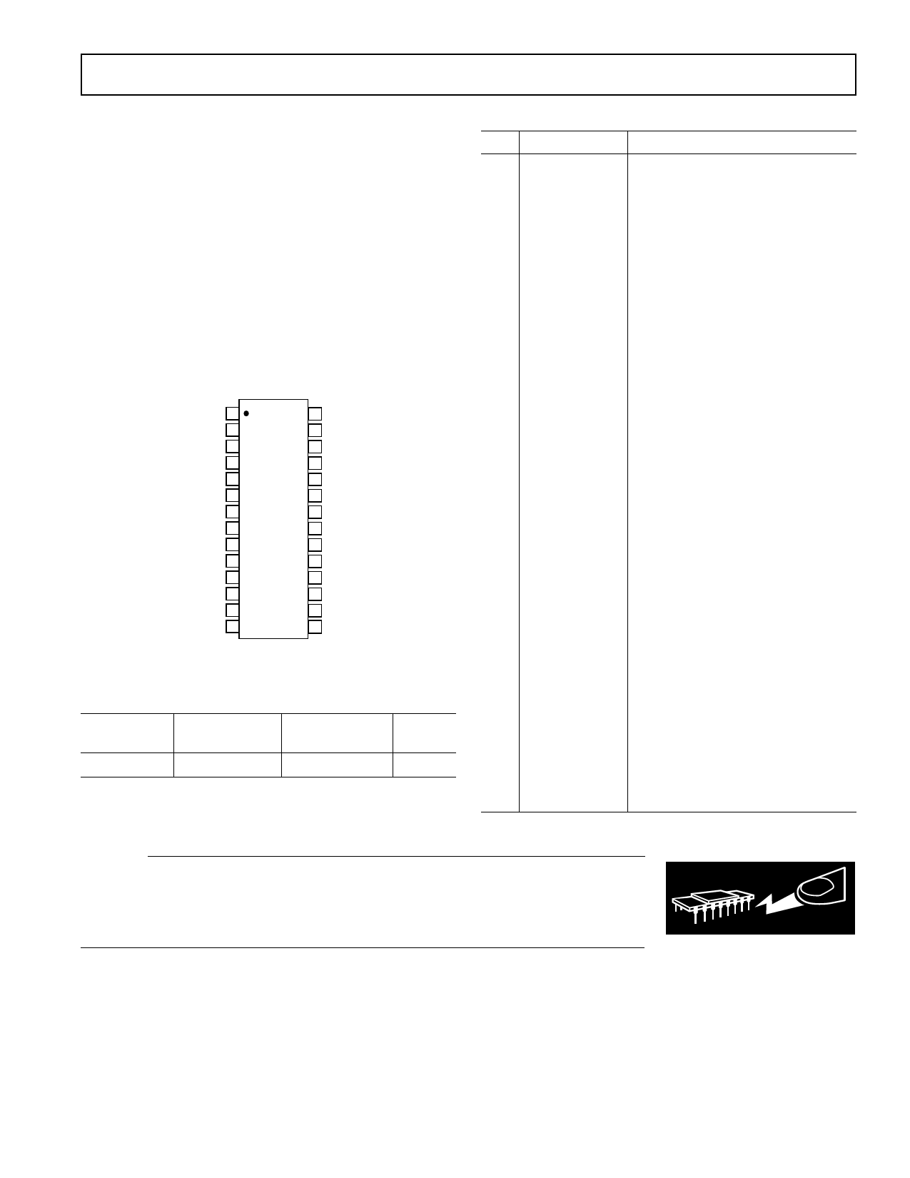
PIN CONFIGURATION
11
12
RESCAP 1
28 CAP+
DGND 2
27 VSIM
13
VTCXO 3
26 CLK
14
RESET 4
25 SIMON
15
REFOUT 5
24 SIMPROG
VCCA 6
23 RST
16
AGND 7 ADP3404 22 I/O
17
VBAT 8 (Not To Scale) 21 SIMGND
VCC 9
20 CLKIN
PWRONKEY 10
19 RESETIN
18
ANALOGON 11
18 DATAIO
PWRONIN 12
17 SIMBAT
19
ROWX 13
16 CAP–
20
CHRON 14
15 VRTC
21
NARROW BODY
TSSOP-28
22
23
ORDERING GUIDE
24
Model
Temperature Package
Range
Description
Package
Option
25
ADP3404ARU –20°C to +85°C 28-Lead TSSOP RU-28
26
27
28
ADP3404
PIN FUNCTION DESCRIPTIONS
Mnemonic
RESCAP
DGND
VTCXO
RESET
REFOUT
VCCA
AGND
VBAT
VCC
PWRONKEY
ANALOGON
PWRONIN
ROWX
CHRON
VRTC
CAP–
SIMBAT
DATAIO
RESETIN
CLKIN
SIMGND
I/O
RST
SIMPROG
SIMON
CLK
VSIM
CAP+
Function
Reset Delay Timing Cap
Digital Ground
Crystal Oscillator Low Dropout
Regulator
Main Reset
Reference Output
Analog Low Dropout Regulator
Analog Ground
Battery Input Voltage
Digital Low Dropout Regulator
Power-On/-Off Key
VTCXO Enable
Power On/Off Signal from
Microprocessor
Microprocessor Keyboard Output
Charger On/Off Input
Real-Time Clock Supply/Coin
Cell Battery Charger
Negative Side of Boost Capacitor
Battery Input for the SIM
Charge Pump
Non-Level-Shifted Bidirectional
Data I/O
Non-Level-Shifted SIM Reset
Non-Level-Shifted Clock
Charge Pump Ground
Level-Shifted Bidirectional SIM
Data Input/Output
Level-Shifted SIM Reset
VSIM Programming:
Low = 3 V, High = 5 V
VSIM Enable
Level-Shifted SIM Clock
SIM Supply
Positive Side of Boost Capacitor
CAUTION
ESD (electrostatic discharge) sensitive device. Electrostatic charges as high as 4000 V readily
accumulate on the human body and test equipment and can discharge without detection.
Although the ADP3404 features proprietary ESD protection circuitry, permanent damage may
occur on devices subjected to high-energy electrostatic discharges. Therefore, proper ESD
precautions are recommended to avoid performance degradation or loss of functionality.
WARNING!
ESD SENSITIVE DEVICE
REV. 0
–5–
Share Link: 