ADP3404 Просмотр технического описания (PDF) - Analog Devices
Номер в каталоге
Компоненты Описание
производитель
ADP3404 Datasheet PDF : 12 Pages
| |||
ADP3404
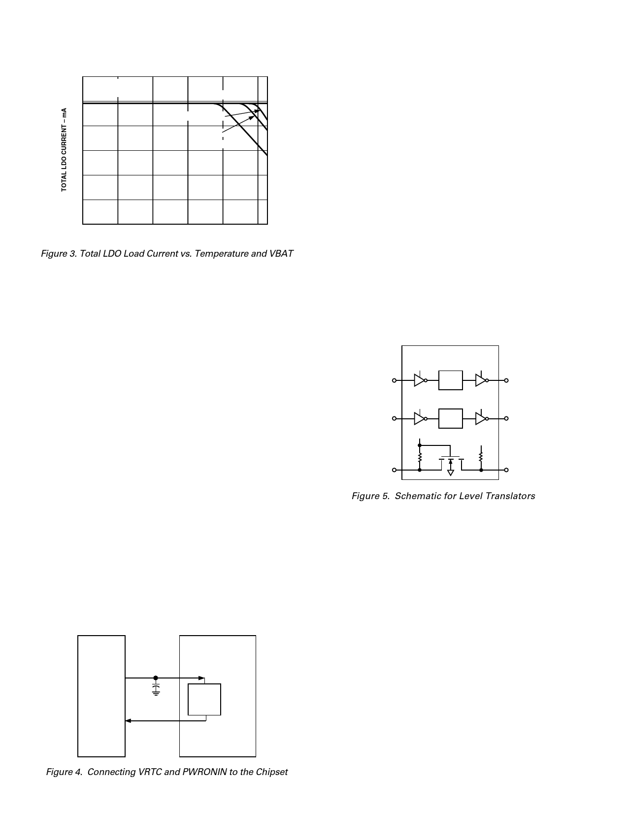
300
6-LAYER BOARD
JA = 62؇C/W
250
200
150
VBAT = 5V
VBAT = 5.5V
VBAT = 6V
VBAT = 7V
100
50
0
؊20
0
20
40
60
80 85
AMBIENT TEMPERATURE – ؇C
Figure 3. Total LDO Load Current vs. Temperature and VBAT
Low Dropout Regulators (LDOs)
The ADP3404 high-performance LDOs are optimized for their
given functions by balancing quiescent current, dropout voltage,
line/load regulation, ripple rejection, and output noise. 2.2 µF
tantalum or MLCC ceramic capacitors are recommended for
use with the digital and analog LDOs, and 0.22 µF for the
TCXO LDO.
Digital LDO (VCC)
The digital LDO (VCC) supplies all the digital circuitry in the
handset (baseband processor, baseband converter, external
memory, display, etc.). The LDO has been optimized for very
low quiescent current (30 µA maximum) at light loads as this
LDO is on at all times.
Analog LDO (VCCA)
This LDO has the same features as the digital LDO. It has further-
more been optimized for good low frequency ripple rejection for use
with analog sections in order to reject the ripple coming from the RF
power amplifier. VCCA is rated to 130 mA load which is sufficient
to supply the complete analog section of a baseband converter such
as the AD6421/AD6425, including a 32 Ω earpiece.
TCXO LDO (VTCXO)
The TCXO LDO is intended as a supply for temperature com-
pensated crystal oscillator, which needs its own ultralow noise
supply. The output current is rated to 5 mA for the TCXO LDO.
RTC LDO (VRTC)
The RTC LDO charges a capacitor-type backup coin cell to run
the real-time clock module. It has been targeted to charge elec-
tric double layer capacitors such as the PAS621 from Kanebo.
The PAS621 has a small physical size (6.8 mm diameter) and a
nominal capacity of 0.3 F, giving many hours of backup time.
ADP3404
GSM PROCESSOR
VRTC
COIN
CELL
PWRONIN
VRTC
RTC
MODULE
PWRON
The ADP3404 supplies current both for charging the coin cell and
for the RTC module when the digital supply is off. The nominal
charging voltage is 2.45 V, which ensures long cell life while obtain-
ing in excess of 90% of the nominal capacity. In addition, it features
a very low quiescent current (10 µA) since this LDO is running all
the time, even when the handset is switched off. It also has reverse
current protection with low leakage which is needed when the main
battery is removed and the coin cell supplies the RTC module.
Reference Output (REFOUT)
The reference output is a low noise, high precision reference with a
guaranteed accuracy of 1.5% over temperature. The reference can
be fed to the baseband converter, such as the AD6425, improving
the absolute accuracy of the converters from 5% to 1.5%. This
significantly reduces calibration time needed for the baseband
converter during production.
SIM Interface
The SIM interface generates the needed SIM voltage—either 3 V
or 5 V, dependent on SIM type, and also performs the needed
logic level translation. Quiescent current is low, as the SIM card
will be powered all the time. Note that DATAIO and I/O have
integrated pull-up resistors as shown in Figure 5. See Table II for
the control logic of the charge pump output, VSIM.
RESETIN
CLKIN
ADP3404
VCC
VSIM
LEVEL
SHIFT
VCC
VCC
LEVEL
SHIFT
VSIM
VSIM
RST
CLK
DATAIO
I/O
Figure 5. Schematic for Level Translators
Power-On/-Off
ADP3404 handles all issues regarding power-on/-off of the hand-
set. It is possible to turn on the ADP3404 in three different ways:
• Pulling PWRONKEY Low
• Pulling PWRONIN High
• CHRON exceeds threshold
Pulling PWRONKEY key low is the normal way of turning on the
handset. This will turn on all the LDOs as long as PWRONKEY is
held low. The microprocessor then starts and pulls PWRONIN
high after which PWRONKEY can be released. PWRONIN going
high will also turn on the handset. This is the case when the alarm
in the RTC module expires.
An external charger can also turn on the phone. The turn-on
threshold and hysteresis can be programmed via external resistors
to allow full flexibility with any external charger and battery chem-
istry. These resistors are referred to as R1 and R2 in Figure 2.
Figure 4. Connecting VRTC and PWRONIN to the Chipset
–10–
REV. 0
Share Link: 