ADNS-7700-HMMY Просмотр технического описания (PDF) - Avago Technologies
Номер в каталоге
Компоненты Описание
производитель
ADNS-7700-HMMY Datasheet PDF : 60 Pages
| |||
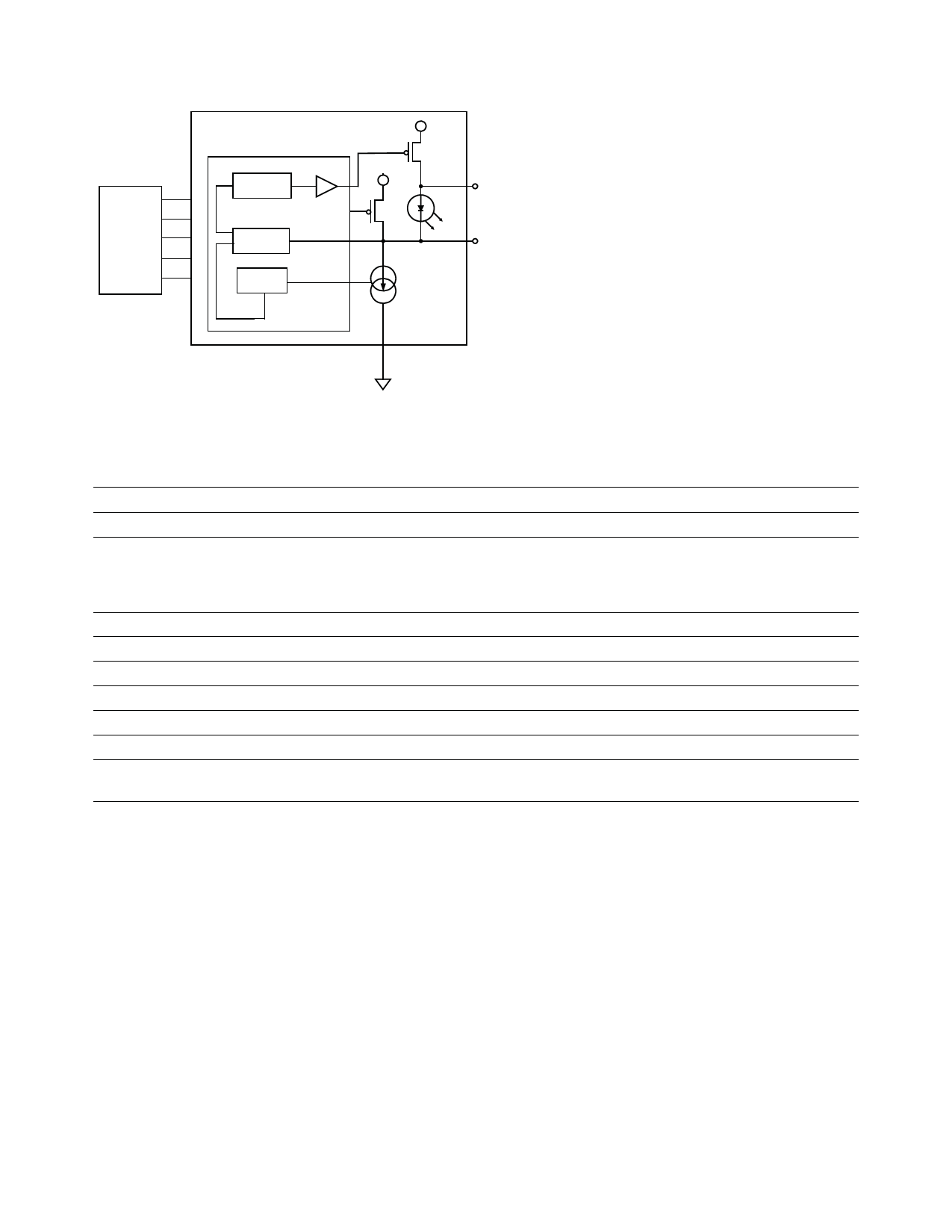
ADNS-7700
LASER
DRIVE
fault control
block
LASER_NEN
VDD3
VDD3
+VCSEL
VCSEL
USB
voltage
Port
sense
XYLASER
VCSEL
current
set
LASER_GND
Figure 8. Single Fault Detection and Eye Safety Feature Block Diagram
Absolute Maximum Ratings
Parameter
Symbol Minimum Maximum Units Notes
Storage Temperature
TS
Lead Solder Temperature
-40
85
260
°C
°C For 7 seconds, 1.6mm below seating plane.
Refer to soldering reflow profile in PCB Assembly
& Soldering Considerations Application Note
AN 5023.
Supply Voltage
ESD
VDD
-0.5
5.5
2
V
kV All pins, human body model
Input Voltage
VIN
-0.5
VDD+0.5
V
All I/O pins except OSC_IN and OSC_OUT, D+, D-
Input Voltage
VIN
-1.0
4.6
V D+, D-, AC waveform, see USB specification (7.1.1)
Input Voltage
VIN
-0.5
3.6
V OSC_IN and OSC_OUT
Input Short Circuit Voltage
VSC
0
VDD
V D+, D-, see USB specification (7.1.1)
Laser Output Power
LOPmax
716
W Class 1 eye safety AEL with ADNS-6180-001 or
ADNS-6180-002 lens
Comments:
1. Stress greater than those listed under “Absolute Maximum Ratings” may cause permanent damage to the device. These are the stress ratings only
and functional operation of the device at these or any other condition beyond those indicated for extended period of time may affect device
reliability.
2. The inherent design of this component causes it to be sensitive to electrostatic discharge. The ESD threshold is listed above. To prevent
ESD-induced damage, take adequate ESD precautions when handling this product.
11
Share Link: 