ADN2873(RevB) Просмотр технического описания (PDF) - Analog Devices
Номер в каталоге
Компоненты Описание
производитель
ADN2873 Datasheet PDF : 20 Pages
| |||
Data Sheet
3.3 V, 50 Mbps to 4.25 Gbps,
Single-Loop, Laser Diode Driver
ADN2873
FEATURES
GENERAL DESCRIPTION
SFP/SFF and SFF-8472 MSA compliant
SFP reference design available
50 Mbps to 4.25 Gbps operation
Automatic average power control
Typical 60 ps output rise/fall time
VCSEL, DFB, and FP laser support
Bias current range: from 2 mA to 100 mA
Modulation current range: from 5 mA to 90 mA
Laser fail alarm and automatic laser shutdown (ALS)
Bias and modulation current monitoring
Voltage setpoint control
Resistor setpoint control
3.3 V supply
24-lead 4 mm × 4 mm LFCSP
Pin compatible with ADN2870
APPLICATIONS
1×/2×/4× Fibre Channel SFP/SFF modules
Multirate OC3 to OC48-FEC SFP/SFF modules
LX-4 modules
DWDM/CWDM laser transmitters
HDTV (SMPTE family) laser transmitters
Like the ADN2870, the ADN2873 laser diode driver (LDD) is
designed for advanced SFP and SFF modules, using SFF-8472
digital diagnostics. The ADN2873 supports NRZ data transmis-
sion operation from 50 Mbps up to 4.25 Gbps. With a new alarm
scheme, this device avoids the shutdown issue caused by the
system transient generated from various lasers.
The ADN2873 monitors the laser bias and modulation currents
and it provides fail alarms and ALS. Using setup voltages of a
microcontroller DAC or a trimmable resistor voltage divider,
the ADN2873 can set up a laser optical average output power and
extinction ratio. The optical average power control loop consists of
an optical feedback from a photodiode, the comparator, and a
status holder. The ADN2873 works easily with the Analog
Devices, Inc., ADuC7019/ADuC7020/ADuC7023 family of
MicroConverter® devices and with the ADN2890/ADN2891/
ADN2892 family of limiting amplifiers to make a complete
SFP/SFF transceiver chipset solution.
The ADN2873 is pin compatible with the ADN2870 dual-loop
LDD, allowing the same design to work with either device. For
dual-loop control applications, refer to the ADN2870 data sheet.
The product is available in a space-saving 24-lead, 4 mm × 4 mm
LFCSP specified over the −40°C to +85°C temperature range.
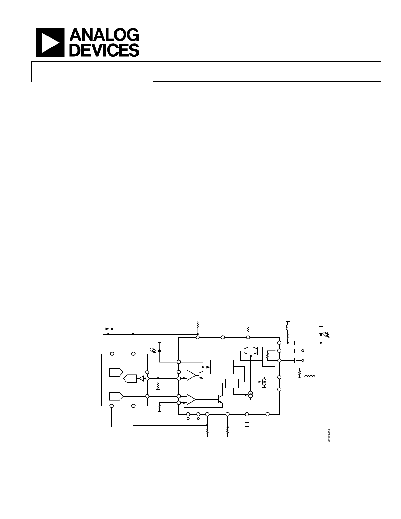
Figure 1 shows an application diagram of the voltage setpoint
control with single-ended laser interface. Figure 36 shows a
differential laser interface.
Tx_DISABLE
Tx_FAULT
APPLICATIONS DIAGRAM
VCC
VCC
VCC
MPD
FAIL
ALS
IMODN
VCC
L
R
IMODP
VCC
LASER
DATAP
ANALOG DEVICES
MICROCONTROLLER
DAC
ADC
DAC
PAVSET
PAVREF
RPAV
1kΩ
GND ERREF
ERSET
1kΩ
GND
CONTROL
×100
IMOD
100Ω
IBIAS
DATAN
VCC
RZ
CCBIAS
ADN2873
VCC GND
IBMON
1kΩ
IMMON PAVCAP DNC
470Ω GND
GND
GND
Figure 1.
Rev. B
Document Feedback
Information furnished by Analog Devices is believed to be accurate and reliable. However, no
responsibility is assumed by Analog Devices for its use, nor for any infringements of patents or other
rights of third parties that may result from its use. Specifications subject to change without notice. No
license is granted by implication or otherwise under any patent or patent rights of Analog Devices.
Trademarks and registered trademarks are the property of their respective owners.
One Technology Way, P.O. Box 9106, Norwood, MA 02062-9106, U.S.A.
Tel: 781.329.4700 ©2008–2016 Analog Devices, Inc. All rights reserved.
Technical Support
www.analog.com
Share Link: 