ADN2872(RevB) Просмотр технического описания (PDF) - Analog Devices
Номер в каталоге
Компоненты Описание
производитель
ADN2872 Datasheet PDF : 20 Pages
| |||

Data Sheet
ABSOLUTE MAXIMUM RATINGS
TA = 25°C, unless otherwise noted.
Table 3.
Parameter
VCC to GND
IMODN, IMODP
PAVCAP, ERCAP, PAVSET, PAVREF, ERREF,
IBIAS, IBMON, IMMON, ALS, CCBIAS,
RPAV, ERSET, FAIL
DATAP, DATAN (Single-Ended Differential)
Junction Temperature (TJ max)
Operating Temperature Range, Industrial
Storage Temperature Range
Power Dissipation (W)1
θJA Thermal Impedance2
θJC Thermal Impedance2
θJB Thermal Impedance2
Rating
4. 2 V
−0.3 V to +4.8 V
−0.3 V to +3.9 V
1.5 V
125°C
−40°C to +85°C
−65°C to +150°C
(TJ max − TA)/θJA
48.6°C/W
5.0°C/W
28.4°C/W
1 Power consumption equations are provided in the Power Consumption section.
2 θJA, θJB, and θJC are estimated when the exposed pad on the device is
soldered on a 4-layer JEDEC board at zero airflow.
ADN2872
Stresses at or above those listed under Absolute Maximum
Ratings may cause permanent damage to the product. This is a
stress rating only; functional operation of the product at these
or any other conditions above those indicated in the operational
section of this specification is not implied. Operation beyond
the maximum operating conditions for extended periods may
affect product reliability.
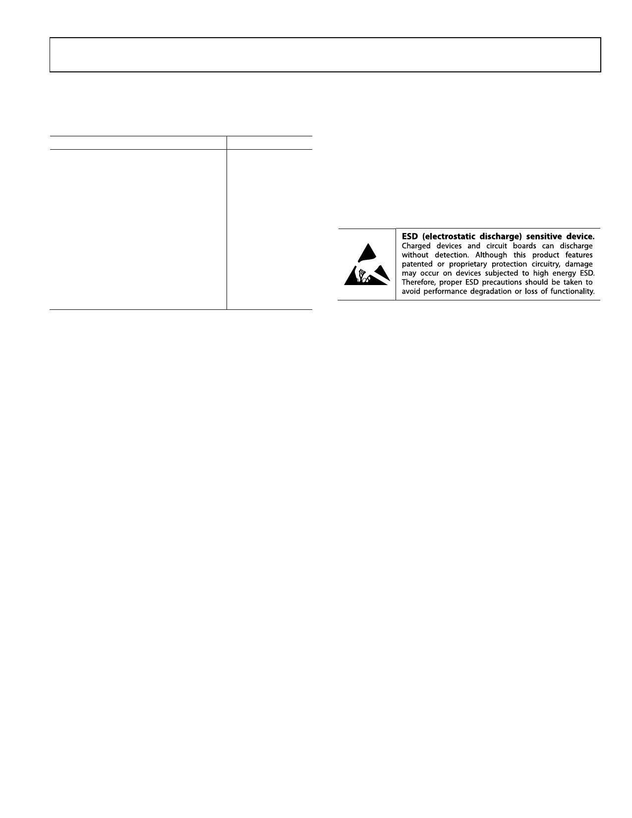
ESD CAUTION
Rev. B | Page 5 of 20