ADN2860(RevB) Просмотр технического описания (PDF) - Analog Devices
Номер в каталоге
Компоненты Описание
производитель
ADN2860 Datasheet PDF : 20 Pages
| |||
ADN2860
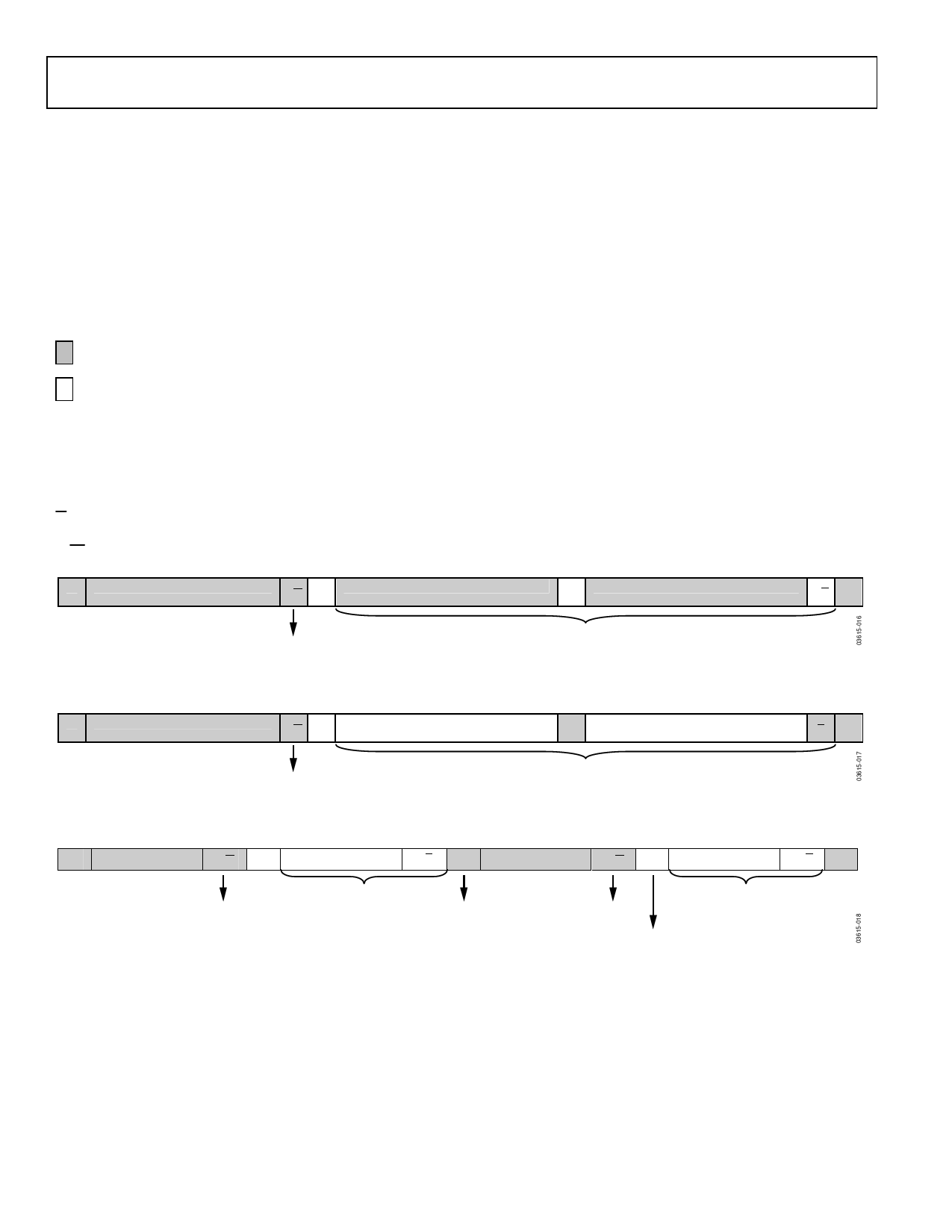
INTERFACE DESCRIPTIONS
I2C INTERFACE
All control and access to both EEPROM memory and the RDAC
registers are conducted via a standard 2-wire I2C interface.
Figure 2 shows the timing characteristics of the I2C bus.
Figure 16 and Figure 17 illustrate standard transmit and receive
bus signals in the I2C interface.
These figures use the following legend:
From master to slave
From slave to master
S = Start condition
P = Stop condition
A = Acknowledge (SDA low)
A = Not acknowledge (SDA high)
R/W = Read enable at high and write enable at low
S
SLAVE ADDRESS
R/W A
DATA
A
DATA
0 = WRITE
DATA TRANSFERRED
(N BYTES + ACKNOWLEDGE)
Figure 16. I2C—Master Transmitting Data to Slave
A/A P
S
SLAVE ADDRESS
R/W A
DATA
A
DATA
1 = WRITE
DATA TRANSFERRED
(N BYTES + ACKNOWLEDGE
Figure 17. I2C—Master Reading Data from Slave
AP
S
SLAVE ADDRESS
R/W
A
DATA
A/A
S
SLAVE ADDRESS
R/W
A
DATA
A/A
P
READ OR WRITE
(N BYTES + ACKNOWLEDGE) REPEATED START
Figure 18. Combined Transmit/Read
READ OR WRITE
(N BYTES + ACKNOWLEDGE)
DIRECTION OF TRANSFER MAY
CHANGE AT THIS POINT
Rev. B | Page 10 of 20
Share Link: 