ADN2814(RevPrA) Просмотр технического описания (PDF) - Analog Devices
Номер в каталоге
Компоненты Описание
производитель
ADN2814
(Rev.:RevPrA)
(Rev.:RevPrA)
Analog Devices

ADN2814 Datasheet PDF : 28 Pages
| |||
ADN2814
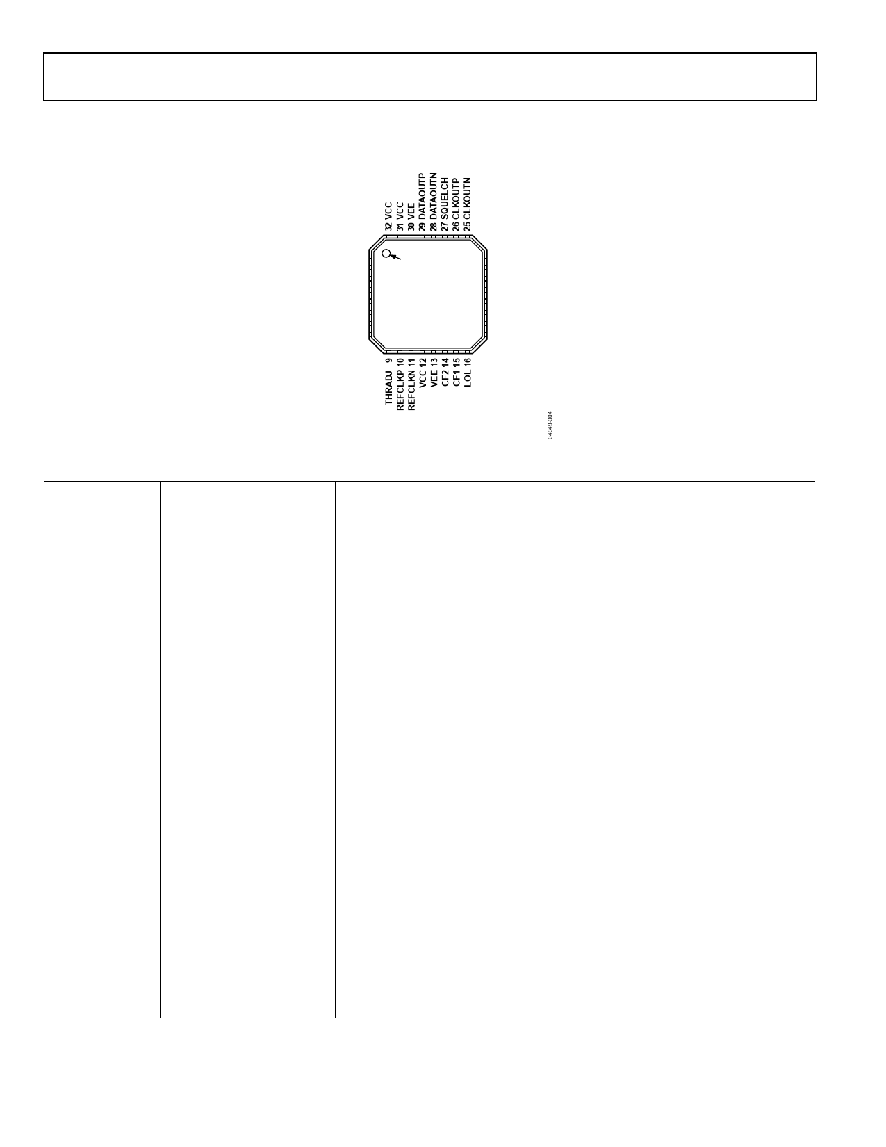
PIN CONFIGURATION AND FUNCTION DESCRIPTIONS
Preliminary Technical Data
TEST1 1
VCC 2
VREF 3
NIN 4
PIN 5
SLICEP 6
SLICEN 7
VEE 8
PIN 1
INDICATOR
ADN2814*
TOP VIEW
(Not to Scale)
24 VCC
23 VEE
22 LOS
21 SDA
20 SCK
19 SADDR5
18 VCC
17 VEE
* THERE IS AN EXPOSED PAD ON THE BOTTOM OF
THE PACKAGE THAT MUST BE CONNECTED TO GND.
Table 5. Pin Function Descriptions
Pin No.
Mnemonic
1
TEST1
2
VCC
3
VREF
4
NIN
5
PIN
6
SLICEP
7
SLICEN
8
VEE
9
THRADJ
10
REFCLKP
11
REFCLKN
12
VCC
13
VEE
14
CF2
15
CF1
16
LOL
17
VEE
18
VCC
19
SADDR5
20
SCK
21
SDA
22
LOS
23
VEE
24
VCC
25
CLKOUTN
26
CLKOUTP
27
SQUELCH
28
DATAOUTN
29
DATAOUTP
30
VEE
31
VCC
32
TEST2
Exposed Pad Pad
Type1
P
AO
AI
AI
AI
AI
P
AI
DI
DI
P
P
AO
AO
DO
P
P
DI
DI
DI
DO
P
P
DO
DO
DI
DO
DO
P
P
P
Figure 4. Pin Configuration
Description
Connect to VCC.
Power for Limamp, LOS.
Internal VREF Voltage. Decouple to GND with a 0.1 µF capacitor.
Differential Data Input. CML.
Differential Data Input. CML.
Differential Slice Level Adjust Input.
Differential Slice Level Adjust Input.
GND for Limamp, LOS.
LOS Threshold Setting Resistor.
Differential REFCLK Input. 12.3 MHz to 200 MHz.
Differential REFCLK Input. 12.3 MHz to 200 MHz.
VCO Power.
VCO GND.
Frequency Loop Capacitor.
Frequency Loop Capacitor.
Loss of Lock Indicator. LVTTL active high.
FLL Detector GND.
FLL Detector Power.
Slave Address Bit 5.
I2C Clock Input.
I2C Data Input.
Loss of Signal Detect Output. Active high. LVTTL.
Output Buffer, I2C GND.
Output Buffer, I2C Power.
Differential Recovered Clock Output. LVDS.
Differential Recovered Clock Output. LVDS.
Disable Clock and Data Outputs. Active high. LVTLL.
Differential Recovered Data Output. LVDS.
Differential Recovered Data Output. LVDS.
Phase Detector, Phase Shifter GND.
Phase Detector, Phase Shifter Power.
Connect to VCC.
Connect to GND
1Type: P = power, AI = analog input, AO = analog output, DI = digital input, DO = digital output.
Rev. PrA | Page 8 of 28
Share Link: