ADM6305 Просмотр технического описания (PDF) - Analog Devices
Номер в каталоге
Компоненты Описание
производитель
ADM6305 Datasheet PDF : 12 Pages
| |||
Data Sheet
FEATURES
Adjustable input threshold voltage options: 0.4 V and 1.23 V
Pretrimmed VCC threshold options (ADM6306)
Increments between 2.5 V and 5 V
Manual reset input (ADM6306)
4 factory programmed reset timeout delays
1 ms, 20 ms, 140 ms, and 1.12 sec (minimum)
Reset output stage: active low, open drain
Low power consumption: 5 µA typical
Power supply glitch immunity
5-lead SOT-23 package
Temperature range: −40°C to +125°C
APPLICATIONS
Portable/battery operated equipment
Microprocessor systems
Multivoltage applications
GENERAL DESCRIPTION
The ADM6305/ADM6306 are dual voltage supervisors designed to
monitor two supplies and provide a reset signal to DSP- and
microprocessor-based systems. Low supply current and a small
form factor make these devices suitable for portable and battery
operated applications.
If a monitored power supply voltage falls below the minimum
voltage threshold, a single active low output asserts triggering a
system reset. After all voltages rise above the selected threshold
level, the reset signal remains low for the reset timeout period.
Four reset timeout options are available.
The ADM6305 monitors two supplies via two adjustable
resistor-programmable undervoltage reset inputs. Both RST
IN1 and RST IN2 have a reset threshold of either 0.4 V or
1.23 V depending on the particular model; that is, the RST IN1
and RST IN2 threshold of the ADM6305D3ARJZ-RL7 model is
Rev. C
Document Feedback
Information furnished by Analog Devices is believed to be accurate and reliable. However, no
responsibility is assumed by Analog Devices for its use, nor for any infringements of patents or other
rights of third parties that may result from its use. Specifications subject to change without notice. No
license is granted by implication or otherwise under any patent or patent rights of Analog Devices.
Trademarks and registered trademarks are the property of their respective owners.
Multiple Input Programmable
Supervisory ICs
ADM6305/ADM6306
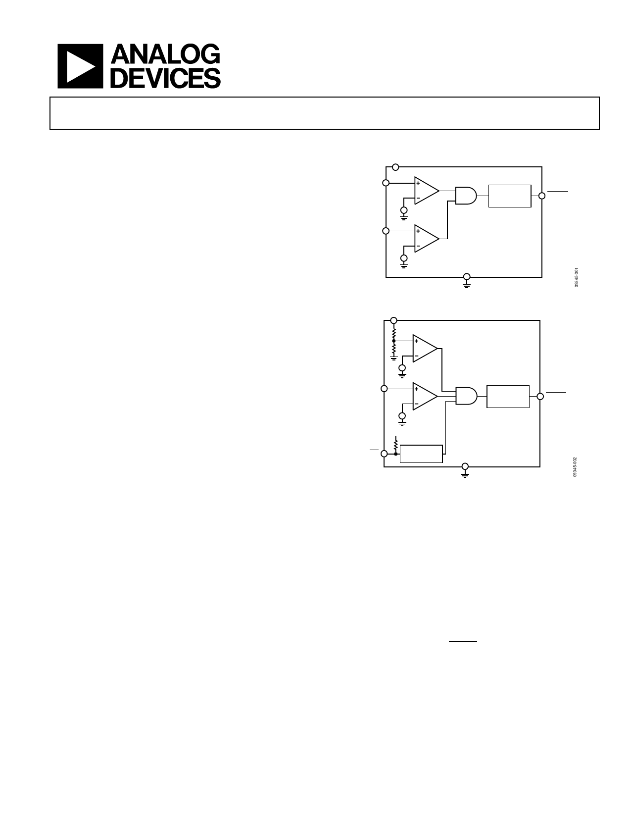
FUNCTIONAL BLOCK DIAGRAMS
VCC
RST IN1
RST IN2
0.4V/1.23V
RESET
GENERATOR
RESET
0.4V/1.23V
ADM6305
GND
Figure 1.
VCC
RST IN
1.23V
0.4V/1.23V
VCC
MR
GLITCH
REJECTION
RESET
GENERATOR
RESET
ADM6306
GND
Figure 2.
1.23 V, while in the case of ADM6305D3ARJZ1-RL7 model, it is
0.4 V. The VCC input of the ADM6305 is not a monitored input.
The ADM6306 has one adjustable undervoltage reset input,
RST IN, which features a choice of reset threshold, 0.4 V or
1.23 V (see the Ordering Guide for more information). The
ADM6306 incorporates a variety of internally pretrimmed VCC
undervoltage threshold options for monitoring supply voltages
in increments between 2.5 V and 5 V. The ADM6306 also
includes a manual reset input. Not all options are released for
sale as standard models. See the Ordering Guide for details.
The ADM6305/ADM6306 RESET output remains valid as long
as VCC exceeds 0.9 V.
The ADM6305/ADM6306 are available in a 5-lead SOT-23
package. These devices are specified over the temperature range
of −40°C to +125°C.
One Technology Way, P.O. Box 9106, Norwood, MA 02062-9106, U.S.A.
Tel: 781.329.4700 ©2010–2018 Analog Devices, Inc. All rights reserved.
Technical Support
www.analog.com
Share Link: 