ADM210 Просмотр технического описания (PDF) - Analog Devices
Номер в каталоге
Компоненты Описание
производитель
ADM210 Datasheet PDF : 12 Pages
| |||
Mnemonic
VCC
V+
V–
GND
C+
C–
C1+
C1–
C2+
C2–
TIN
TOUT
RIN
ROUT
EN/EN
SD/SD
NC
ADM205–ADM211/ADM213
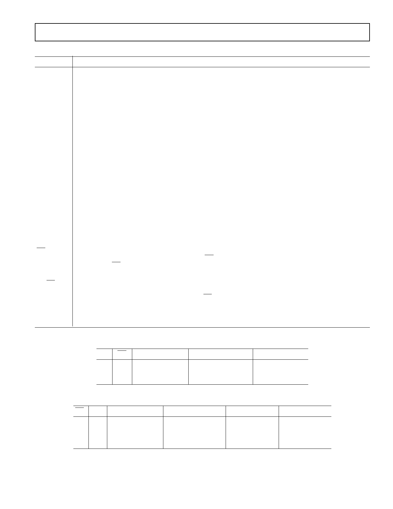
PIN FUNCTION DESCRIPTION
Function
Power Supply Input 5 V ± 10% (+5 V ± 5% ADM205).
Internally generated positive supply (+10 V nominal) on all parts except ADM209.
ADM209 requires external 9 V to 13.2 V supply.
Internally generated negative supply (–10 V nominal).
Ground pin. Must be connected to 0 V.
(ADM209 only) External capacitor (+ terminal) is connected to this pin.
(ADM209 only) External capacitor (– terminal) is connected to this pin.
(ADM206, ADM207, ADM208, ADM211, ADM213) External capacitor (+ terminal) is connected to this pin.
(ADM206, ADM207, ADM208, ADM211, ADM213) External capacitor (– terminal) is connected to this pin.
(ADM206, ADM207, ADM208, ADM211, ADM213) External capacitor (+ terminal) is connected to this pin.
(ADM206, ADM207, ADM208, ADM211, ADM213) External capacitor (– terminal) is connected to this pin.
Transmitter (Driver) Inputs. These inputs accept TTL/CMOS levels. An internal 400 kΩ pull-up resistor to Vcc is
connected on each input.
Transmitter (Driver) Outputs. These are RS-232 levels (typically ± 10 V).
Receiver Inputs. These inputs accept RS-232 signal levels. An internal 5 kΩ pull-down resistor to GND is con-
nected on each input.
Receiver Outputs. These are TTL/CMOS levels.
Enable Input. Active low on ADM205, ADM206, ADM209, ADM211. Active high on ADM213. This input is
used to enable/disable the receiver outputs. With EN = Low (EN = High ADM213), the receiver outputs are en-
abled. With EN =High (EN = low ADM213), the outputs are placed in a high impedance state. This facility is
useful for connecting to microprocessor systems.
Shutdown Input. Active high on ADM205, ADM206, ADM211. Active low on ADM213. With SD = high on the
ADM205, ADM206, ADM211, the charge pump is disabled, the receiver outputs are placed in a high impedance
state and the driver outputs are turned off. With SD low on the ADM213, the charge pump is disabled, the driver
outputs are turned off and all receivers except R4 and R5 are placed in a high impedance state. In shutdown, the
power consumption reduces to 5 µW.
No Connect. No connections are required to this pin.
Table II. ADM205, ADM206, ADM211 Truth Table
SD EN Status
Transmitters T1–T5 Receivers R1–R5
0
0
Normal Operation Enabled
0
1
Normal Operation Enabled
1
0
Shutdown
Disabled
Enabled
Disabled
Disabled
SD EN
00
01
10
11
Table III. ADM213 Truth Table
Status
Transmitters T1-T4 Receivers R1-R3 Receivers R4, R5
Shutdown
Shutdown
Normal Operation
Normal Operation
Disabled
Disabled
Enabled
Enabled
Disabled
Disabled
Disabled
Enabled
Disabled
Enabled
Disabled
Enabled
REV. 0
–7–
Share Link: 