ADM1487AR Просмотр технического описания (PDF) - Analog Devices
Номер в каталоге
Компоненты Описание
производитель
ADM1487AR
Analog Devices

ADM1487AR Datasheet PDF : 8 Pages
| |||
ADM1487
PRELIMINARY TECHNICAL DATA
CMOS outout stages, which include parasitic diodes from
their driver outputs to each supply rail and can latch up
when these diodes conduct.
VCC
SCHOTTKY
R E V E R S E -B IA S E D
WHEN OUTPUT
> VCC+VD
PARASITIC
DIODE DP
PARASITIC
DIODE DP
SCHOTTKY
R E V E R S E -B IA S E D
WHEN OUTPUT
< GND - VD
Figure 9. ADM1487 Driver Output Stage
The ADM1487 output includes Schottky diodes in series
with the positive supply to the drain of the P-channel output
device and in series with the drain of the N-channel output
device. These diodes prevent the P-channel's parasitic diode
from conducting when the output voltage exceeds VCC and
prevent the N-channel's parasitic diode from conducting
when the output voltage falls below ground.
SLEW RATE CONTROL
The driver output stage of the ADM1487 has a controlled
slew rate to minmize signal reflections on incorrectly termi-
nated lines and to reduce electromagnetic interference (EMI).
CURRENT LIMIT AND THERMAL SHUTDOWN
The ADM1487 incorporates two protection mechanisms to
guard the drivers against short-circuits, bus contention or
other fault conditions. The first is a current-limited output
stage that protects the driver against short-circuits over the
entire common-mode voltage range by limiting the output
current to about 70mA. Under extreme fault condtions
where the current limit is not effective, a thermal shutdown
circuit puts the driver outputs into a high-impedance state if
the die temperature exceeds 150°C, and does not turn them
back on until the temperature has fallen to 130°C.
ENHANCED ESD PROTECTION
All Analog Devices parts incorporate protection against
electrostatic discharge (ESD) to protect the devices dur-
ing handling, assembly and normal operation. In addition,
the ADM1487 has enhanced ESD protection up to ±10kV
on the A and B I/O pins to protect against severe opera-
tional conditions such as line transients, connection and
disconnection.
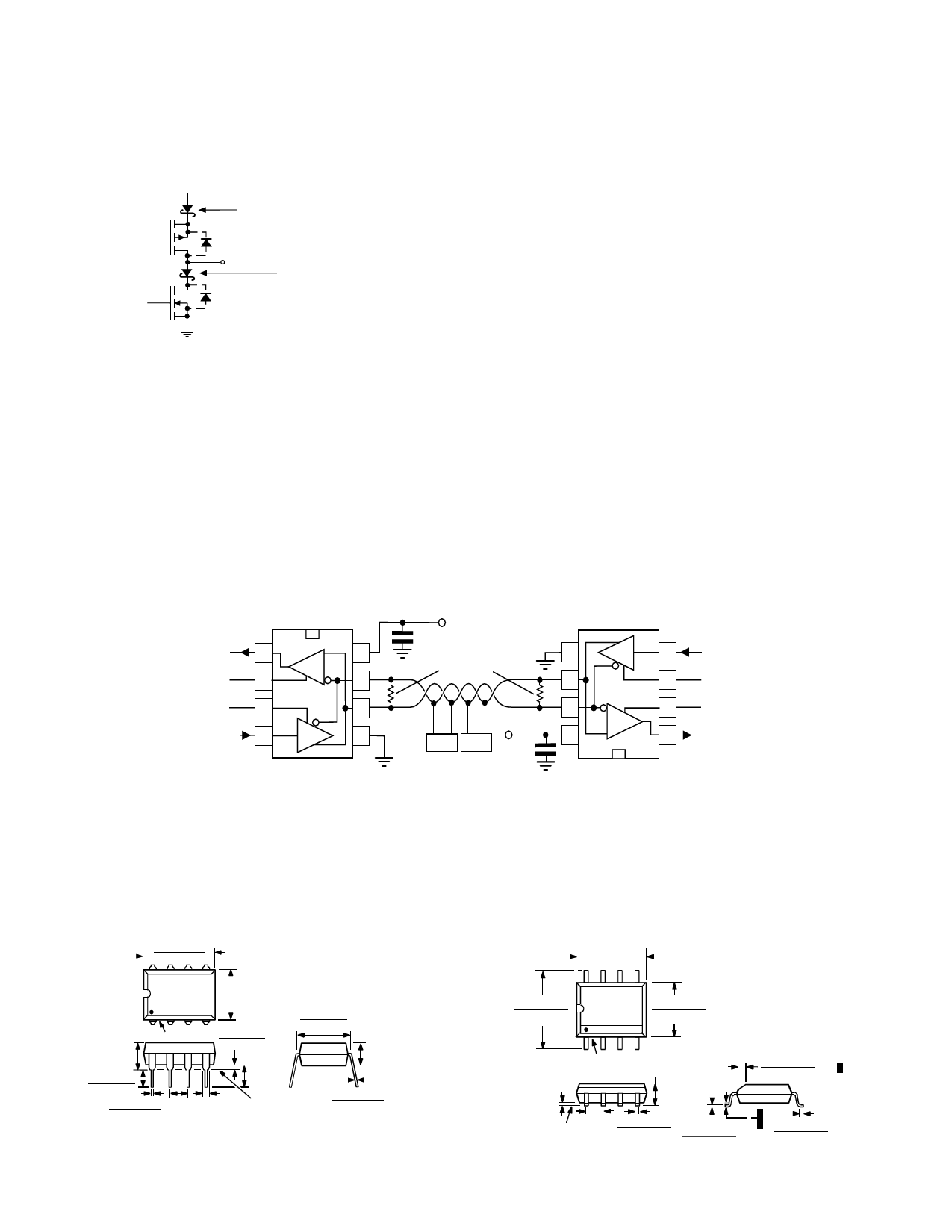
APPLICATION INFORMATION
Figure 10 shows a typical application of the ADM1487.
This is a half-duplex RS-485/RS-422 network. Up to 254
additional ADM1487s can be connected along the cable
(termination resistors are only required at each end).
+5V
RECEIVER
OUTPUT
1
(RO)
RECEIVER
ENABLE
2
DRI(VREER)
3
R
8
7B
RT
6
100n (VCC
)
CABLE TERMINATED
AT ENDS
5
6
RT
7
D
4
DI
3
DE
2
RE
ENABLE
A
DA(DTEA)
4
D
5
IN (DI)
+5V (VCC) 8
R
B A B A 100n
1
RO
ADM1487
ADDITIONAL
ADM1487s
ADM1487
Figure 10. Typical Half-Duplex RS-485/RS-422 Network
OUTLINE DIMENSIONS
Dimensions shown in inches and (mm).
8-Pin Plastic Dual-In-Line Package (N-8)
8-Pin SO Package (R-8)
0.430 (10.92)
0.348 (8.84)
8
5
0.280 (7.11)
0.240 (6.10)
14
0.325 (8.25)
PIN 1
0.060 (1.52)
0.300 (7.62)
0.210 (5.33)
0.015 (0.38)
MAX
0.130
0.160 (4.06)
0.115 (2.93)
(3.30)
MIN
0.022 (0.558) 0.100 0.070 (1.77)
0.014 (0.356) (2.54) 0.045 (1.15)
BSC
SE A TIN G
PLANE
0.195 (4.95)
0.115 (2.93)
0.015 (0.381)
0.008 (0.204)
0.1968 (5.00)
0.1890 (4.80)
85
0.244 0 (6.20)
0.228 4 (5.80) 1
0.1574 (4.00)
4 0.1497 (3.80)
PIN 1
0.102 (2.59)
0.094 (2.39)
0.0196 (0.50)
x 45
0.0099 (0.25)
0.009 8 (0 .25)
0.004 0 (0 .10)
8
0.0500 0.0192 (0.49)
0
SE A TIN G (1.27) 0.0138 (0.35) 0.0098 (0.25)
PLANE BSC
0.0075 (0.19)
0.05 00 (1 .27)
0.01 60 (0 .41)
–8–
Rev. PrC
Share Link: