ADL5353 Просмотр технического описания (PDF) - Analog Devices
Номер в каталоге
Компоненты Описание
производитель
ADL5353 Datasheet PDF : 24 Pages
| |||
2200 MHz to 2700 MHz Balanced Mixer,
LO Buffer, IF Amplifier, and RF Balun
ADL5353
FEATURES
Frequency ranges of 2200 MHz to 2700 MHz (RF) and 30 MHz
to 450 MHz (IF)
Power conversion gain: 8.7 dB
Input IP3 of 24.5 dBm and Input P1dB of 10.4 dBm
SSB noise figure of 9.8 dB
Typical LO drive of 0 dBm
Single-ended, 50 Ω RF and LO input ports
High isolation SPDT LO input switch
Single-supply operation: 3.3 V to 5 V
Exposed pad, 5 mm × 5 mm 20-lead LFCSP
1500 V HBM/500 V FICDM ESD performance
APPLICATIONS
Cellular base station receivers
Transmit observation receivers
Radio link downconverters
GENERAL DESCRIPTION
The ADL5353 uses a highly linear, doubly balanced passive
mixer core along with integrated RF and local oscillator (LO)
balancing circuitry to allow for single-ended operation. The
ADL5353 incorporates an RF balun to provide optimal perfor-
mance over a 2200 MHz to 2700 MHz input frequency range
using high-side LO. The balanced passive mixer arrangement
provides good LO-to-RF leakage, typically better than −36 dBm,
and excellent intermodulation performance.
The balanced mixer core also provides extremely high input
linearity, allowing the device to be used in demanding cellular
applications where in-band blocking signals might otherwise
result in the degradation of dynamic performance. A high
linearity IF buffer amplifier follows the passive mixer core to yield a
typical power conversion gain of 8.8 dB and can be used with a
wide range of output impedances.
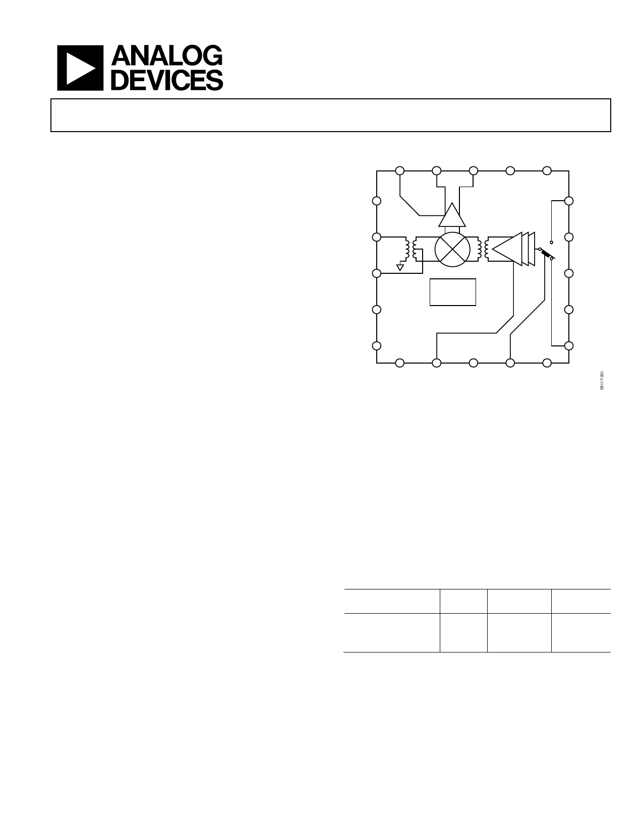
FUNCTIONAL BLOCK DIAGRAM
IFGM
20
IFOP
19
IFON
18
PWDN
17
LEXT
16
VPIF 1
ADL5353
15 LOI2
RFIN 2
14 VPSW
RFCT 3
COMM 4
BIAS
GENERATOR
13 VGS1
12 VGS0
COMM 5
11 LOI1
6
7
8
9
10
VLO3
LGM3
VLO2
LOSW
NC
NC = NO CONNECT
Figure 1.
The ADL5353 provides two switched LO paths that can be used
in TDD applications where it is desirable to rapidly switch between
two local oscillators. LO current can be externally set using a
resistor to minimize dc current commensurate with the desired
level of performance. For low voltage applications, the ADL5353 is
capable of operation at voltages down to 3.3 V with substantially
reduced current. For low voltage operation, an additional logic
pin is provided to power down (<200 µA) the circuit when desired.
The ADL5353 is fabricated using a BiCMOS high performance
IC process. The device is available in a 5 mm × 5 mm, 20-lead
LFCSP and operates over a −40°C to +85°C temperature range.
An evaluation board is also available.
Table 1. Passive Mixers
Single
RF Frequency (MHz) Mixer
500 to 1700
ADL5367
1200 to 2500
ADL5365
2200 to 2700
Single Mixer
and IF Amp
ADL5357
ADL5355
ADL5353
Dual Mixer
and IF Amp
ADL5358
ADL5356
ADL5354
Rev. 0
Information furnished by Analog Devices is believed to be accurate and reliable. However, no
responsibility is assumed by Analog Devices for its use, nor for any infringements of patents or other
rights of third parties that may result from its use. Specifications subject to change without notice. No
license is granted by implication or otherwise under any patent or patent rights of Analog Devices.
Trademarks and registered trademarks are the property of their respective owners.
One Technology Way, P.O. Box 9106, Norwood, MA 02062-9106, U.S.A.
Tel: 781.329.4700
www.analog.com
Fax: 781.461.3113
©2010 Analog Devices, Inc. All rights reserved.
Share Link: 