ADIS16265 Просмотр технического описания (PDF) - Analog Devices
Номер в каталоге
Компоненты Описание
производитель
ADIS16265 Datasheet PDF : 20 Pages
| |||
Data Sheet
PIN CONFIGURATION AND FUNCTION DESCRIPTIONS
VREF GND GND VCC VCC
SCLK
DOUT
DIN
CS
DIO1
20
1
2
3
19 18 17
ADIS16260/
ADIS16265
TOP VIEW
(Not to Scale)
16
15
14
13
POSITIVE OUTPUT
4
ROTATIONAL
12
DIRECTION
5
11
6 7 8 9 10
FILT
RATE
AUX
ADC
AUX
DAC
DNC
DIO2 RST DNC DNC DNC
NOTES
1. DNC = DO NOT CONNECT.
2. THE PINS CANNOT BE SEEN FROM THE TOP.
THIS LOOK-THOUGH VIEW OF THEIR LOCATION
IS OFFERED FOR REFERENCE IN DEVELOPING
PCB PATTERNS.
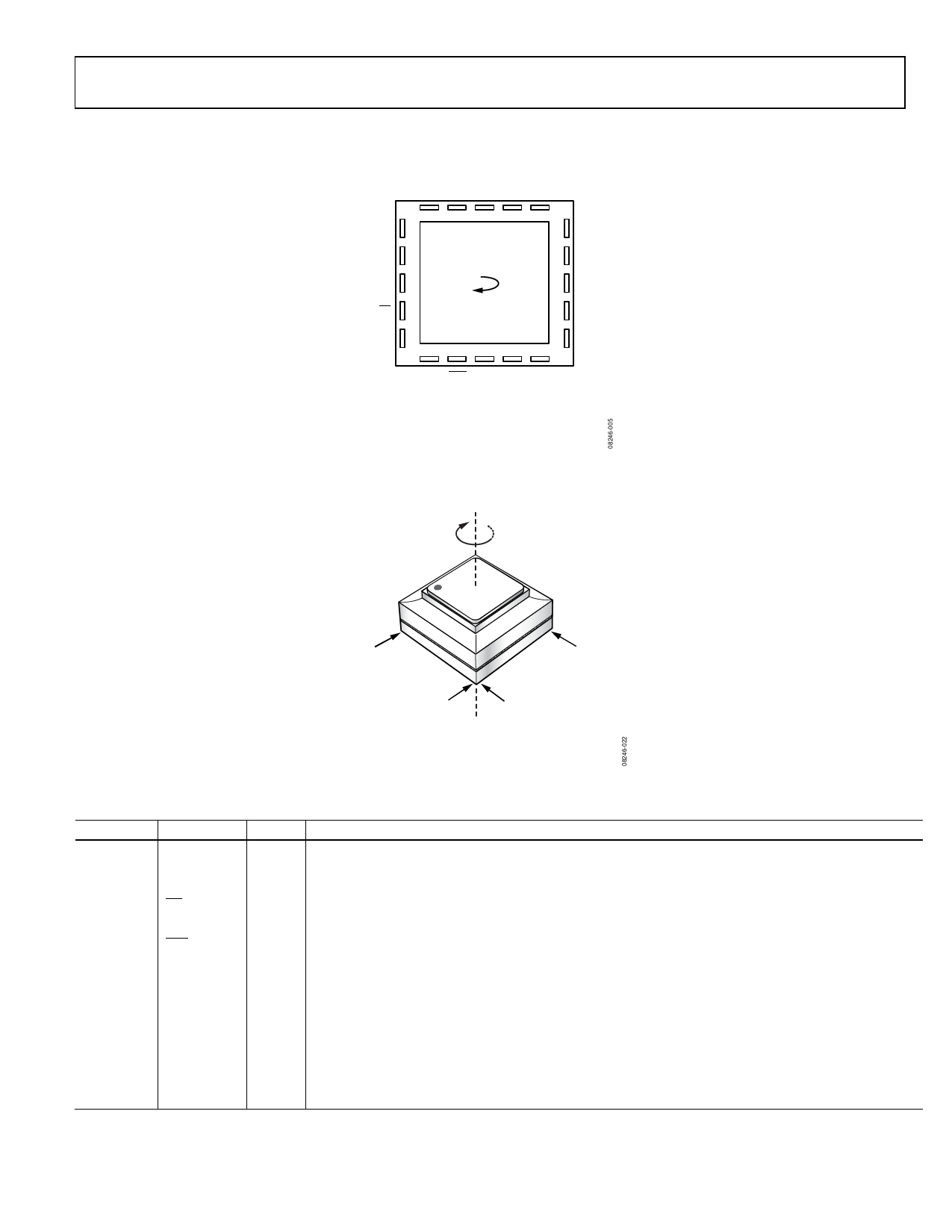
Figure 4. Pin Configuration
AXIS OF ROTATION
ADIS16260/ADIS16265
PIN 1
PIN 10
PIN 5
PIN 6
NOTES
1. ARROW INDICATES THE DIRECTION OF ROTATION
THAT PRODUCES A POSITIVE RESPONSE IN
THE GYRO_OUT REGISTER.
Figure 5. Axial Orientation
Table 4. Pin Function Descriptions
Pin No.
Mnemonic Type1
1
SCLK
I
2
DOUT
O
3
DIN
I
4
CS
I
5, 6
DIO1, DIO2 I/O
7
RST
I
8, 9, 10, 11 DNC
12
AUX DAC O
13
AUX ADC I
14
RATE
O
15
FILT
I
16, 17
VCC
S
18, 19
GND
S
20
VREF
O
Description
SPI Serial Clock.
SPI Data Output. Clocks output on SCLK falling edge.
SPI Data Input. Clocks input on SCLK rising edge.
SPI Chip Select. Active low.
Configurable Digital Input/Output.
Reset. Active low.
Do Not Connect.
Auxiliary DAC Output.
Auxiliary ADC Input.
Rate Output. For bandwidth reduction only; output is not specified.
Filter Terminal.
5.0 V Power Supply.
Ground.
Precision Reference Output.
1 I = input, I/O = input/output, O = output, S = supply.
Rev. D | Page 7 of 20
Share Link: 