ADIS16265ACCZ(RevPrA) Просмотр технического описания (PDF) - Analog Devices
Номер в каталоге
Компоненты Описание
производитель
ADIS16265ACCZ Datasheet PDF : 19 Pages
| |||
Preliminary Technical Data
ADIS16260/ADIS16265
PIN CONFIGURATION AND FUNCTION DESCRIPTIONS
VREF COM COM VCC VCC
SCLK
DOUT
DIN
CS
DIO0
20
1
2
3
19 18 17
ADIS16250/
ADIS16255
TOP VIEW
(Not To Scale)
16
15
14
13
POSITIVE OUTPUT
4
ROTATIONAL
12
DIRECTION
5 DNC = DO NOT CONNECT 11
6 7 8 9 10
FILT
RATE
AUX
ADC
AUX
DAC
DNC
DIO1 RST DNC DNC DNC
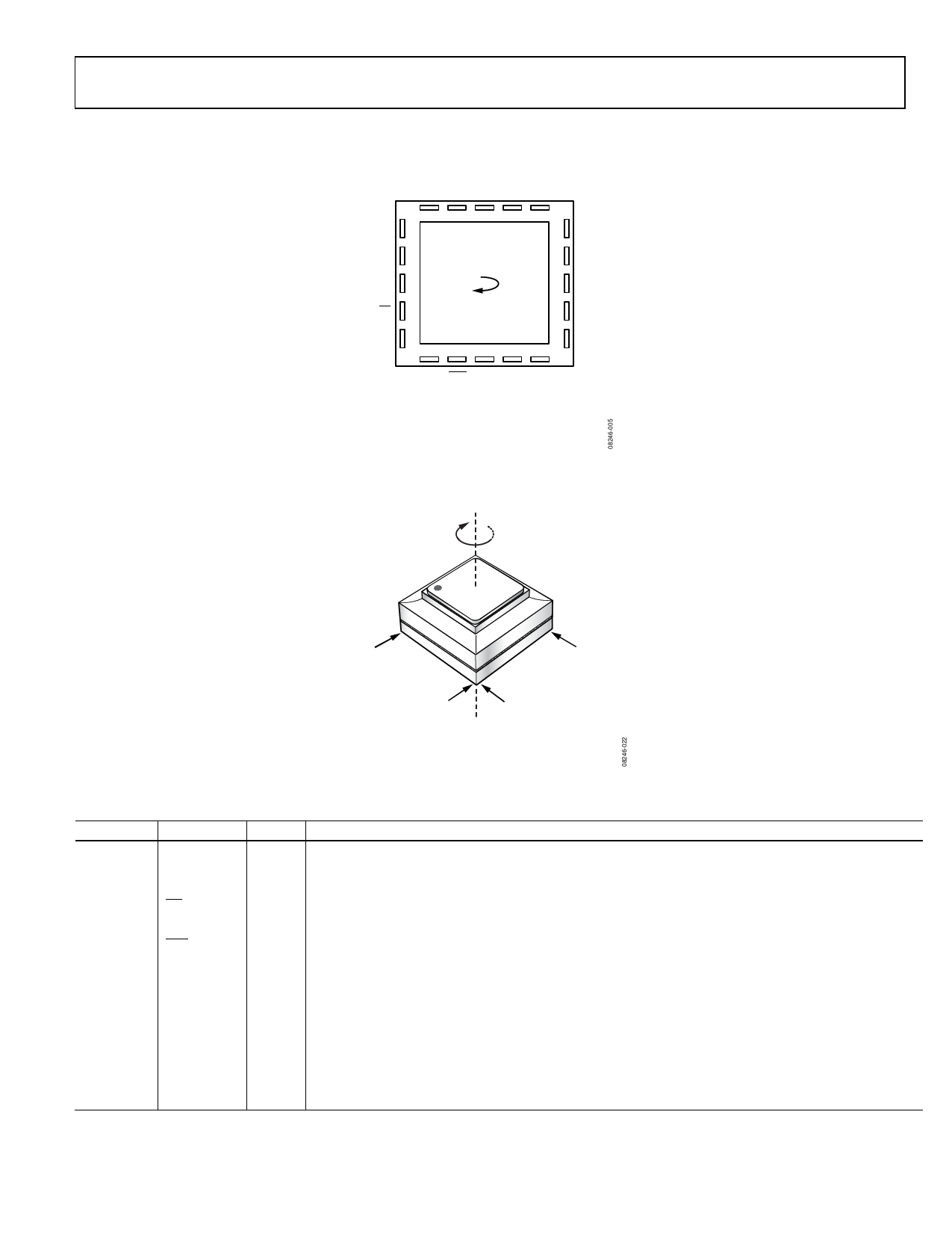
Figure 5. Pin Configuration
Table 4. Pin Function Descriptions
Pin No.
Mnemonic Type1
1
SCLK
I
2
DOUT
O
3
DIN
I
4
CS
I
5, 6
DIO0, DIO1 I/O
7
RST
I
8, 9, 10, 11 DNC
–
12
AUX DAC O
13
AUX ADC I
14
RATE
O
15
FILT
I
16, 17
VCC
S
18, 19
COM
S
20
VREF
O
Description
SPI, Serial Clock.
SPI, Data Output.
SPI, Data Input.
SPI, Chip Select, Active Low.
Multifunction Digital Input/Output Pin.
Reset, Active Low. This resets the sensor signal conditioning circuit and initiates a start-up sequence.
Do Not Connect.
Auxiliary DAC Analog Output Voltage.
Auxiliary ADC Analog Input Voltage.
Analog Rate Signal Output (Uncalibrated).
Analog Amplifier Summing Junction. This is used for setting the analog bandwidth. See the Analog
Bandwidth section for more details.
5.0 V Power Supply.
Common. Reference point for all circuitry in the ADIS16260/ADIS16265.
Precision Reference Output.
1 S = supply; O = output; I = input.
RECOMMENDED LAYOUT
3.800
8×
5.0865
8×
0.773
16×
10.173 7.600
2×
4×
0.500
20×
1.127
20×
11mm × 11mm STACKED LGA PACKAGE
Figure 6. Recommended Pad Layout (Units in Millimeters)
Rev. PrA | Page 7 of 19
Share Link: 