ADF7011 Просмотр технического описания (PDF) - Analog Devices
Номер в каталоге
Компоненты Описание
производитель
ADF7011 Datasheet PDF : 24 Pages
| |||
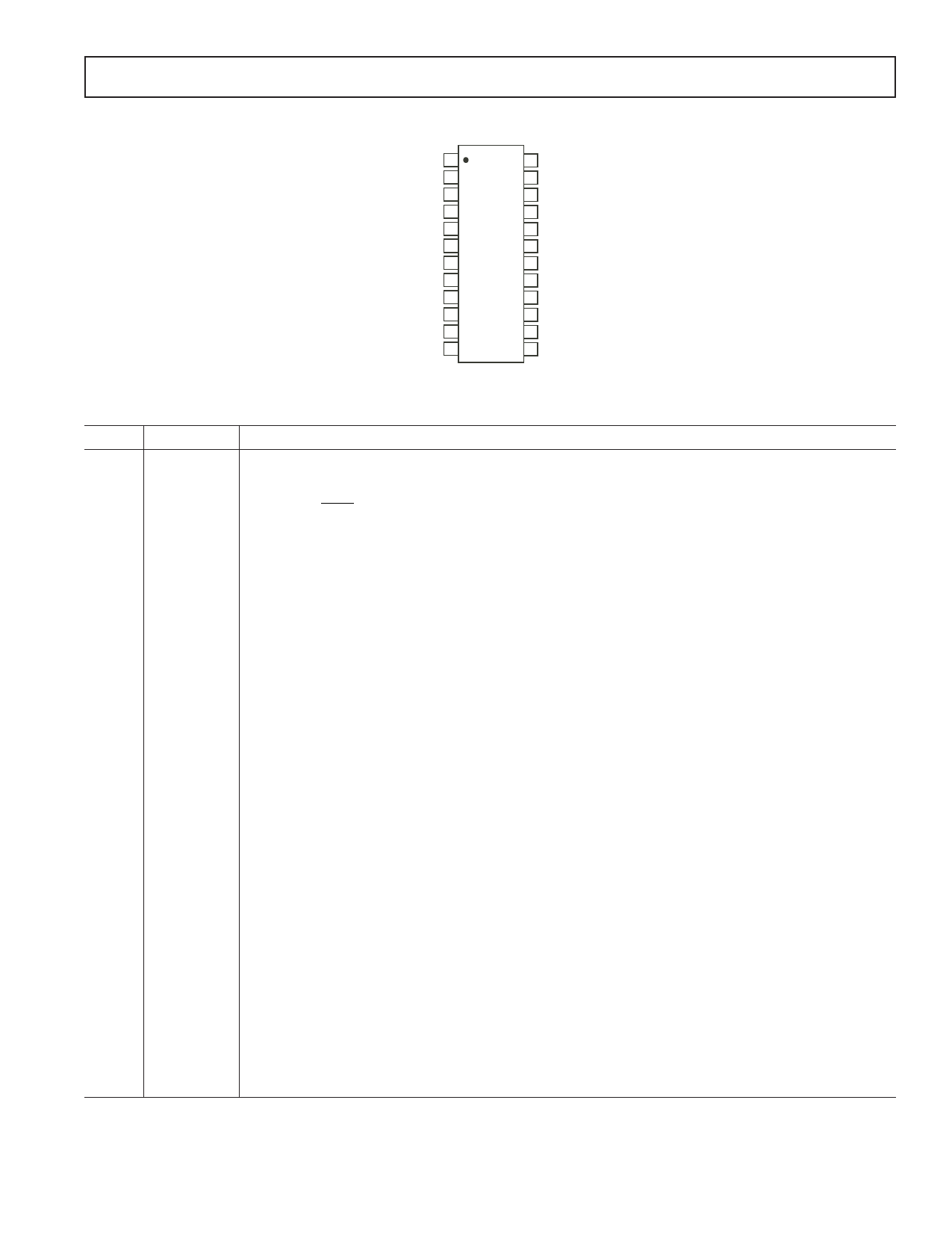
PIN CONFIGURATION
RSET 1
24 CREG
CPVDD 2
23 CVCO
CPGND 3
CPOUT 4
TSSOP
22 VCOIN
21 AGND
CE 5 ADF7011 20 RFOUT
DATA 6 TOP VIEW 19 RFGND
CLK 7 (Not to Scale) 18 DVDD
LE 8
17 TEST
TxDATA 9
TxCLK 10
16 VCOGND
15 OSC1
MUXOUT 11
14 OSC2
DGND 12
13 CLKOUT
ADF7011
Pin No. Mnemonic
1
RSET
2
CPVDD
3
CPGND
4
CPOUT
5
CE
6
DATA
7
CLK
8
LE
9
TxDATA
10
TxCLK
11
MUXOUT
12
DGND
13
CLKOUT
14
OSC2
PIN FUNCTION DESCRIPTIONS
Function
External Resistor to Set Change Pump Current and Some Internal Bias Currents. Use 4.7 kΩ as default:
ICP MAX
=
9.5
RSET
So, with RSET = 4.7 kΩ, ICP MAX = 2.02 mA.
Charge Pump Supply. This should be biased at the same level as RFOUT and DVDD. The pin should be
decoupled with a 0.1 µF capacitor as close to the pin as possible.
Charge Pump Ground.
Charge Pump Output. This output generates current pulses that are integrated in the loop filter. The
integrated current changes the control voltage on the input to the VCO.
Chip Enable. A logic low applied to this pin powers down the part. This must be high for the part to
function. This is the only way to power down the regulator circuit.
Serial Data Input. The serial data is loaded MSB first with the two LSBs being the control bits. This is a
high impedance CMOS input.
Serial Clock Input. This serial clock is used to clock in the serial data to the registers. The data is latched
into the 24-bit shift register on the CLK rising edge. This input is a high impedance CMOS input.
Load Enable, CMOS Input. When LE goes high, the data stored in the shift registers is loaded into one
of the four latches, the latch being selected using the control bits.
Digital data to be transmitted is input on this pin.
GFSK Only. This clock output is used to synchronize microcontroller data to the TxDATA pin of the
ADF7011. The clock is provided at the same frequency as the data rate.
This multiplexer output allows either the digital lock detect (most common), the scaled RF, or the scaled
reference frequency to be accessed externally. Used commonly for system debug. See the Function Regis-
ter Map.
Ground Pin for the RF Digital Circuitry.
The Divided Down Crystal Reference with 50:50 Mark-Space Ratio. May be used to drive the clock
input of a microcontroller. To reduce spurious components in the output spectrum, the sharp edges can
be reduced with a series RC. For 4.8 MHz output clock, a series 50 Ω into 10 pF will reduce spurs to
< –50 dBc. Defaults on power-up to divide by 16.
Oscillator Pin. If a single-ended reference (such as a TCXO) is used, it should be applied to this pin.
When using an external signal generator, a 51 Ω resistor should be tied from this pin to ground. The
XOE bit in the R register should set high when using an external reference.
REV. 0
–5–
Share Link: 