ADF4157BRUZ Просмотр технического описания (PDF) - Analog Devices
Номер в каталоге
Компоненты Описание
производитель
ADF4157BRUZ Datasheet PDF : 24 Pages
| |||
ADF4157
PHASE FREQUENCY DETECTOR (PFD) AND
CHARGE PUMP
The PFD takes inputs from the R counter and the N counter
and produces an output proportional to the phase and fre-
quency difference between them. Figure 14 is a simplified
schematic of the phase frequency detector. The PFD includes
a fixed delay element that sets the width of the antibacklash
pulse, which is typically 3 ns. This pulse ensures that there is no
dead zone in the PFD transfer function and gives a consistent
reference spur level.
UP
HI
D1 Q1
U1
+IN
CLR1
DELAY
U3
CHARGE
PUMP
CP
HI
–IN
CLR2 DOWN
D2 Q2
U2
Figure 14. PFD Simplified Schematic
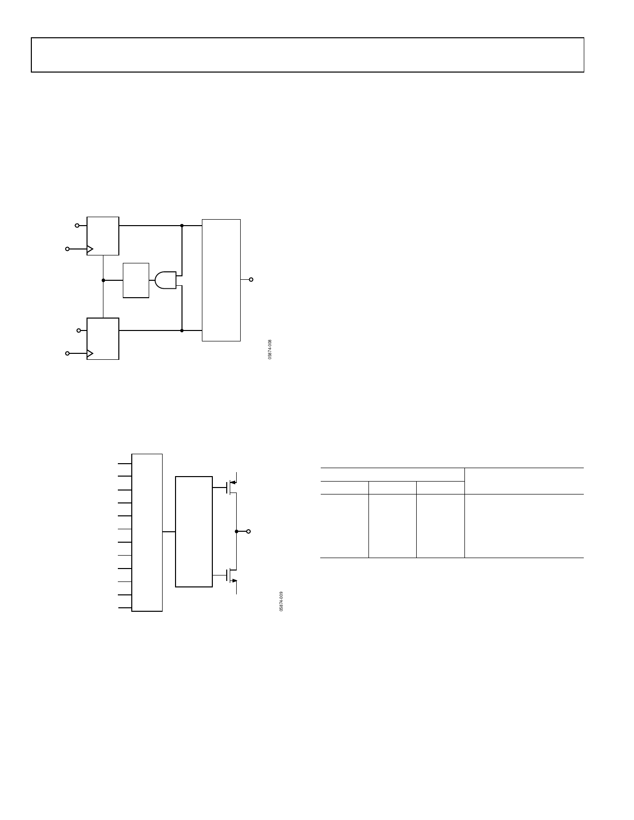
MUXOUT AND LOCK DETECT
The output multiplexer on the ADF4157 allows the user to access
various internal points on the chip. The state of MUXOUT is
controlled by M4, M3, M2, and M1 (see Figure 17). Figure 15
shows the MUXOUT section in block diagram form.
THREE-STATE OUTPUT
DVDD
DGND
R DIVIDER OUTPUT
N DIVIDER OUTPUT
ANALOG LOCK DETECT
DIGITAL LOCK DETECT
MUX
CONTROL
SERIAL DATA OUTPUT
CLK DIVIDER OUTPUT
FASTLOCK SWITCH
R DIVIDER/2
N DIVIDER/2
Figure 15. MUXOUT Schematic
DVDD
MUXOUT
DGND
Data Sheet
INPUT SHIFT REGISTER
The ADF4157 digital section includes a 5-bit RF R counter, a
12-bit RF N counter, and a 25-bit FRAC counter. Data is clocked
into the 32-bit input shift register on each rising edge of CLK.
The data is clocked in MSB first. Data is transferred from the
input shift register to one of five latches on the rising edge of
LE. The destination latch is determined by the state of the three
control bits (C3, C2, and C1) in the input shift register. These
are the three LSBs, DB2, DB1, and DB0, as shown in Figure 2.
The truth table for these bits is shown in Table 6. Figure 16
shows a summary of how the latches are programmed.
PROGRAM MODES
Table 6 and Figure 16 through Figure 21 show how to set up
the program modes in the ADF4157.
Several settings in the ADF4157 are double-buffered. These
include the LSB FRAC value, R counter value, reference doubler,
and current setting. This means that two events have to occur
before the part uses a new value of any of the double-buffered
settings. First, the new value is latched into the device by writing to
the appropriate register. Second, a new write must be performed
on Register 0, R0.
For example, updating the fractional value can involve a write
to the 13 LSB bits in R1 and the 12 MSB bits in R0. R1 should
be written to first, followed by the write to R0. The frequency
change begins after the write to R0. Double buffering ensures
that the bits written to in R1 do not take effect until after the
write to R0.
Table 6. C3, C2, and C1 Truth Table
Control Bits
C3
C2
C1
Register
0
0
0
Register 0 (R0)
0
0
1
Register 1 (R1)
0
1
0
Register 2 (R2)
0
1
1
Register 3 (R3)
1
0
0
Register 4 (R4)
Rev. D | Page 10 of 24
Share Link: 