ADCMP580BCPZ-WP(RevB) Просмотр технического описания (PDF) - Analog Devices
Номер в каталоге
Компоненты Описание
производитель
ADCMP580BCPZ-WP Datasheet PDF : 16 Pages
| |||
ADCMP580/ADCMP581/ADCMP582
Data Sheet
VTP 1
VP 2
VN 3
VTN 4
ADCMP582
TOP VIEW
12 VCCO
11 Q
10 Q
9 VCCO
NOTES
1. THE METALLIC BACK SURFACE OF THE PACKAGE IS NOT ELECTRICALLY
CONNECTED TO ANY PART OF THE CIRCUIT. IT CAN BE LEFT FLOATING FOR
OPTIMAL ELECTRICAL ISOLATION BETWEEN THE PACKAGE HANDLE AND
THE SUBSTRATE OF THE DIE. IT CAN ALSO BE SOLDERED TO THE
APPLICATION BOARD IF IMPROVED THERMAL AND/OR MECHANICAL
STABILITY IS DESIRED.
Figure 4. ADCMP582 Pin Configuration
Table 5. ADCMP582 Pin Function Descriptions
Pin No. Mnemonic Description
1
VTP
Termination Resistor Return Pin for VP Input.
2
VP
Noninverting Analog Input.
3
VN
Inverting Analog Input.
4
VTN
Termination Resistor Return Pin for VN Input.
5, 16
VCCI
6
LE
Positive Supply Voltage.
Latch Enable Input Pin, Inverting Side. In compare mode (LE = low), the output tracks changes at the input of the
comparator. In latch mode (LE = high), the output reflects the input state just prior to the comparator being
placed into latch mode. LE must be driven in complement with LE.
7
LE
Latch Enable Input Pin, Noninverting Side. In compare mode (LE = high), the output tracks changes at the input
of the comparator. In latch mode (LE = low), the output reflects the input state just prior to the comparator being
placed into latch mode. LE must be driven in complement with LE.
8
VTT
Termination Return Pin for the LE/LE Input Pins. For the ADCMP582 (PECL output stage), connect this pin to the
VCCO –2 V termination potential.
9, 12
VCCO
10
Q
Digital Ground Pin/Positive Logic Power Supply Terminal. This pin must be connected to the positive logic power
VCCO supply.
Inverting Output. Q is logic low if the analog voltage at the noninverting input, VP, is greater than the analog
voltage at the inverting input, VN, provided that the comparator is in compare mode. See the LE/LE descriptions
(Pin 6 to Pin 7) for more information.
11
Q
Noninverting Output. Q is logic high if the analog voltage at the noninverting input, VP, is greater than the analog
voltage at the inverting input, VN, provided that the comparator is in compare mode. See the LE/LE descriptions
(Pin 6 to Pin 7) for more information.
13
VEE
Negative Power Supply.
14
HYS
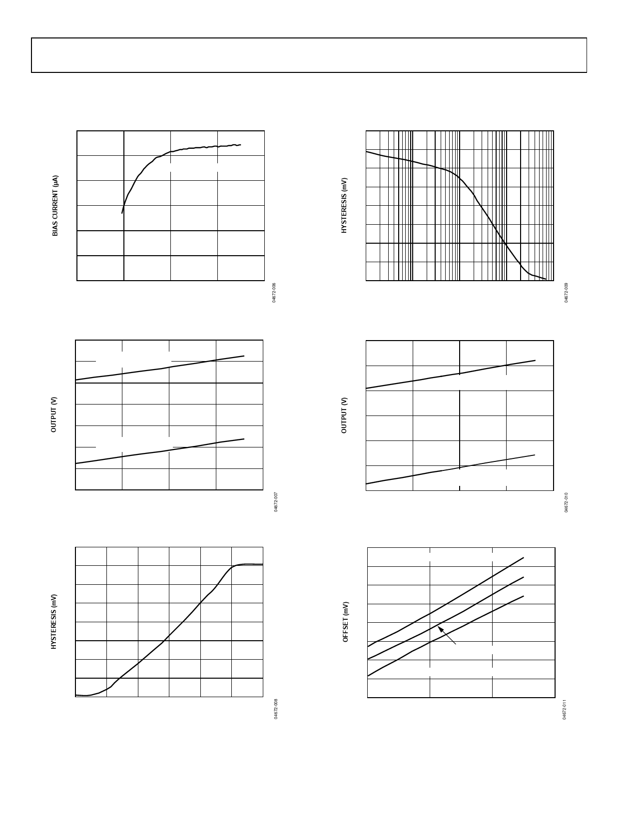
Hysteresis Control. Leave this pin disconnected for zero hysteresis. Connect this pin to the VEE supply with a
suitably sized resistor to add the desired amount of hysteresis. Refer to Figure 8 for proper sizing of the HYS
hysteresis control resistor.
15
GND
Analog Ground.
EPAD
Exposed Pad. The metallic back surface of the package is not electrically connected to any part of the circuit. It
can be left floating for optimal electrical isolation between the package handle and the substrate of the die. It
can also be soldered to the application board if improved thermal and/or mechanical stability is desired.
Rev. B | Page 8 of 16
Share Link: 