AD9755 –ü—Ä–æ—Å–º–æ—Ç—Ä —Ç–µ—Ö–Ω–∏—á–µ—Å–∫–æ–≥–æ –æ–ø–∏—Å–∞–Ω–∏—è (PDF) - Analog Devices
–ù–æ–º–µ—Ä –≤ –∫–∞—Ç–∞–ª–æ–≥–µ
–ö–æ–º–ø–æ–Ω–µ–Ω—Ç—ã –û–ø–∏—Å–∞–Ω–∏–µ
–ø—Ä–æ–∏–∑–≤–æ–¥–∏—Ç–µ–ª—å
AD9755 Datasheet PDF : 28 Pages
| |||
AD9755
FUNCTIONAL DESCRIPTION
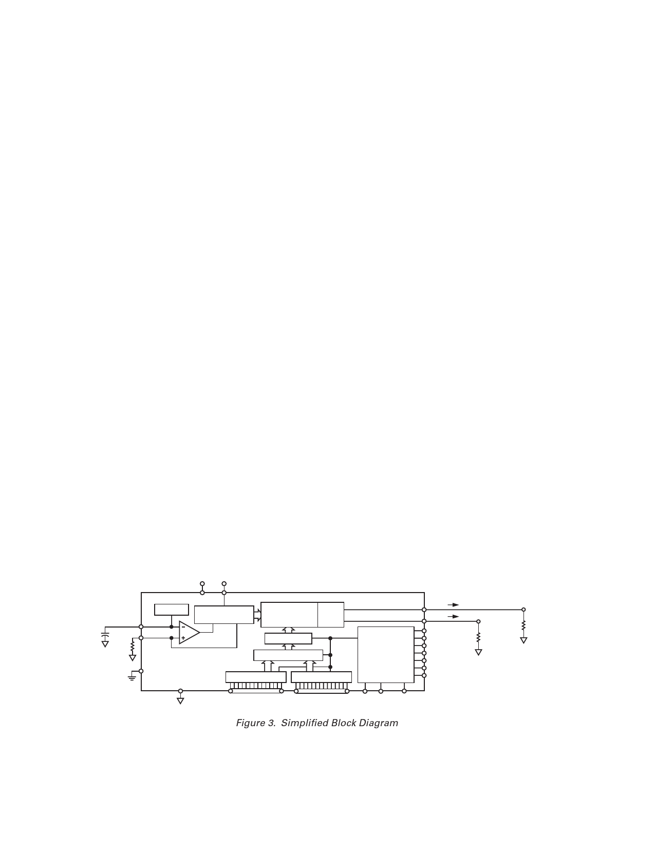
Figure 3 shows a simplified block diagram of the AD9755. The
AD9755 consists of a PMOS current source array capable of
providing up to 20 mA of full-scale current, IOUTFS. The array is
divided into 31 equal sources that make up the five most significant
bits (MSBs). The next four bits, or middle bits, consist of 15 equal
current sources whose value is 1/16th of an MSB current source.
The remaining LSBs are a binary weighted fraction of the middle
bit current sources. Implementing the middle and lower bits
with current sources, instead of an R-2R ladder, enhances dynamic
performance for multitone or low amplitude signals and helps
maintain the DAC’s high output impedance (i.e., >100 kΩ).
All of the current sources are switched to one or the other of the
two outputs (i.e., IOUTA or IOUTB) via PMOS differential current
switches. The switches are based on a new architecture that
significantly improves distortion performance. This new switch
architecture reduces various timing errors and provides matching
complementary drive signals to the inputs of the differential
current switches.
The analog and digital sections of the AD9755 have separate
power supply inputs (i.e., AVDD and DVDD) that can operate
independently over a 3.0 V to 3.6 V range. The digital section,
which is capable of operating at a 300 MSPS clock rate, consists
of edge-triggered latches and segment decoding logic circuitry.
The analog section includes the PMOS current sources, the
associated differential switches, a 1.20 V band gap voltage
reference, and a reference control amplifier.
The full-scale output current is regulated by the reference
control amplifier and can be set from 2 mA to 20 mA via an
external resistor, RSET. The external resistor, in combination
with both the reference control amplifier and voltage reference
VREFIO, sets the reference current IREF, which is replicated to the
segmented current sources with the proper scaling factor. The
full-scale current, IOUTFS, is 32 times the value of IREF.
REFERENCE OPERATION
The AD9755 contains an internal 1.20 V band gap reference.
This can easily be overdriven by an external reference with no
effect on performance. REFIO serves as either an input or output,
depending on whether the internal or an external reference is used.
To use the internal reference, simply decouple the REFIO
pin to ACOM with a 0.1 µF capacitor. The internal reference
voltage will be present at REFIO. If the voltage at REFIO is
to be used elsewhere in the circuit, an external buffer amplifier
with an input bias current less than 100 nA should be used. An
example of the use of the internal reference is given in Figure 4.
A low impedance external reference can be applied to REFIO, as
shown in Figure 5. The external reference may provide either a
fixed reference voltage to enhance accuracy and drift performance
or a varying reference voltage for gain control. Note that the 0.1 µF
compensation capacitor is not required since the internal reference
is overdriven, and the relatively high input impedance of REFIO
minimizes any loading of the external reference.
REFERENCE CONTROL AMPLIFIER
The AD9755 also contains an internal control amplifier that is
used to regulate the DAC’s full-scale output current, IOUTFS.
The control amplifier is configured as a voltage-to-current con-
verter as shown in Figure 4, so that its current output, IREF, is
determined by the ratio of VREFIO and an external resistor, RSET,
as stated in Equation 4. IREF is applied to the segmented current
sources with the proper scaling factor to set IOUTFS, as stated in
Equation 3.
The control amplifier allows a wide (10:1) adjustment span of
IOUTFS over a 2 mA to 20 mA range by setting IREF between
62.5 µA and 625 µA. The wide adjustment span of IOUTFS provides
several application benefits. The first benefit relates directly to
the power dissipation of the AD9755, which is proportional to
IOUTFS (refer to the Power Dissipation section). The second
benefit relates to the 20 dB adjustment, which is useful for sys-
tem gain control purposes.
The small signal bandwidth of the reference control amplifier is
approximately 500 kHz and can be used for low frequency, small
signal multiplying applications.
0.1␮F
RSET
2k⍀
3.0V TO 3.6V
1.2V REF
REFIO
DVDD AVDD
PMOS CURRENT
SOURCE ARRAY
FSADJ
SEGMENTED
SWITCHES FOR
DB0 TO DB13
DAC
DAC LATCH
AD9755
DCOM
ACOM
2 –1 MUX
PORT 1 LATCH
PORT 2 LATCH
DB0 – DB13
DB0 – DB13
DIGITAL DATA INPUTS
PLL
CIRCUITRY
VDIFF = VOUTA – VOUTB
IOUTA
IOUTB
PLLVDD
CLKVDD
CLK+
CLK–
CLKCOM
RESET
LPF
VOUT B
RLOAD
50⍀
VOUT A
RLOAD
50⍀
DIV0 DIV1 PLLLOCK
Figure 3. Simplified Block Diagram
–10–
REV. B
Share Link: 