AD8189 Просмотр технического описания (PDF) - Analog Devices
Номер в каталоге
Компоненты Описание
производитель
AD8189 Datasheet PDF : 24 Pages
| |||
AD8188/AD8189
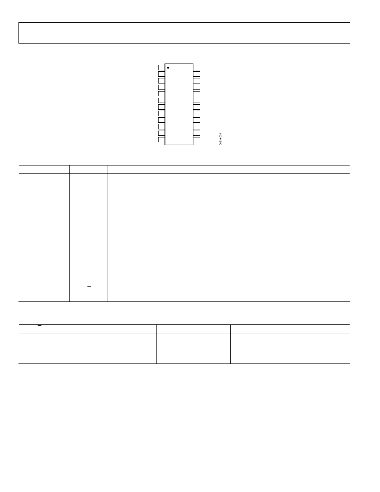
PIN CONFIGURATION AND FUNCTION DESCRIPTIONS
IN0A 1
DGND 2
24 VCC
23 OE
IN1A 3
22 SEL A/B
VREF 4
IN2A 5
AD8188/ 21 VCC
AD8189 20 OUT0
VCC 6 TOP VIEW 19 VEE
VEE
7
(Not to Scale)
18 OUT1
IN2B 8
VEE 9
17 VCC
16 OUT2
IN1B 10
VEE 11
15 VEE
14 DVCC
IN0B 12
13 VCC
Figure 4. AD8188/AD8189 Pin Configuration
Table 4. Pin Function Descriptions
Pin No.
Mnemonic Description
1
IN0A
Input, High-ZIN. Routed to OUT0 when A is selected.
2
DGND
Ground Reference for Digital Control Circuitry.
3
IN1A
Input, High-ZIN. Routed to OUT1 when A is selected.
4
VREF
AD8188: Bypass point for internal reference. Does not affect dc level of output.
AD8189: Input to reference buffers for all channels. Can be used to offset the outputs.
5
6, 13, 17, 21, 24
7, 9, 11, 15, 19
8
10
12
14
16
IN2A
VCC
VEE
IN2B
IN1B
IN0B
DVCC
OUT2
Input, High-ZIN. Routed to OUT2 when A is selected.
Positive Analog Supply. Nominally 5 V higher than VEE.
Negative Analog Supply.
Input, High-ZIN. Routed to OUT2 when B is selected.
Input, High-ZIN. Routed to OUT1 when B is selected.
Input, High-ZIN. Routed to OUT0 when B is selected.
Positive Supply for Digital Control Circuitry. Referenced to DGND.
Output. Can connect to IN2A, IN2B, or disable.
18
OUT1
Output. Can connect to IN1A, IN1B, or disable.
20
OUT0
Output. Can connect to IN0A, IN0B, or disable.
22
SEL A/B
Logic high selects the three A inputs. Logic low selects the three B inputs.
23
OE
Output Enable. Logic high enables the three outputs.
Table 5. Truth Table
SEL A/B
0
1
1
0
OE
OUT
0
High-Z
0
High-Z
1
INxA
1
INxB
Rev. 0 | Page 6 of 24
Share Link: 