AD7818ARM-REEL Просмотр технического описания (PDF) - Analog Devices
Номер в каталоге
Компоненты Описание
производитель
AD7818ARM-REEL Datasheet PDF : 20 Pages
| |||
Data Sheet
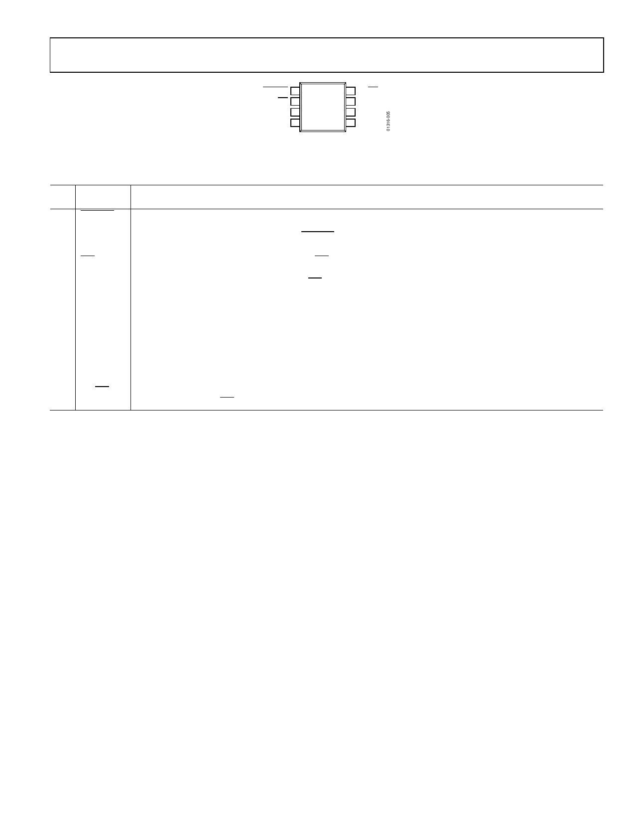
CONVST 1
8 RD/WR
OTI 2 AD7818 7 SCLK
TOP VIEW
GND 3 (Not to Scale) 6 DIN/OUT
VIN 4
5 VDD
Figure 5. AD7818 Pin Configuration
AD7817/AD7818
Table 5. AD7818 Pin Function Descriptions
Pin
No. Mnemonic Description
1 CONVST
Logic Input Signal. The convert start signal initiates a 10-bit analog-to-digital conversion on the falling edge of this
signal. The falling edge of this signal places track-and-hold in hold mode. Track-and-hold goes into track mode again at
the end of the conversion. The state of the CONVST signal is checked at the end of a conversion. If it is logic low, the
AD7818 powers down. See the Operating Modes section.
2 OTI
Logic Output. The overtemperature indicator (OTI) is set logic low if the result of a conversion on Channel 0
(temperature sensor) is greater that an 8-bit word in the overtemperature register (OTR). The signal is reset at the end
of a serial read operation, that is, a rising RD/WR edge.
3 GND
Analog and Digital Ground.
4
VIN
Analog Input Channel. The input channel is single-ended with respect to GND. The input channel can convert voltage
signals in the range 0 V to 2.5 V. The input channel is selected by writing to the address register of the AD7818. See the
Control Byte section.
5
VDD
6
DIN/OUT
7 SCLK
Positive Supply Voltage, 2.7 V to 5.5 V.
Logic Input and Output. Serial data is clocked in and out of the AD7818 at this pin.
Clock Input for the Serial Port. The serial clock is used to clock data into and out of the AD7818. Data is clocked out on
the falling edge and clocked in on the rising edge.
8 RD/WR
Logic Input. The read/write signal is used to indicate to the AD7818 whether the next data transfer operation is a read
or a write. Set the RD/WR logic high for a read operation and logic low for a write.
Rev. D | Page 9 of 20
Share Link: 