AD7538(RevA) Просмотр технического описания (PDF) - Analog Devices
Номер в каталоге
Компоненты Описание
производитель
AD7538 Datasheet PDF : 8 Pages
| |||
AD7538
TERMINOLOGY
RELATIVE ACCURACY
Relative accuracy or endpoint nonlinearity is a measure of the
maximum deviation from a straight line passing through the
endpoints of the DAC transfer function. It is measured after ad-
justing for zero error and full-scale error and is normally ex-
pressed in Least Significant Bits or as a percentage of full-scale
reading.
DIFFERENTIAL NONLINEARITY
Differential nonlinearity is the difference between the measured
change and the ideal 1 LSB change between any two adjacent
codes. A specified differential nonlinearity of ± 1 LSB max over
the operating temperature range ensures monotonicity.
GAIN ERROR
Gain error is a measure of the output error between an ideal
DAC and the actual device output. It is measured with all 1s in
the DAC after offset error has been adjusted out and is expressed
in Least Significant Bits. Gain error is adjustable to zero with an
external potentiometer.
DIGITAL-TO-ANALOG GLITCH IMPULSE
The amount of charge injected from the digital inputs to the
analog output when the inputs change state is called Digital-
to-Analog Glitch Impulse. This is normally specified as the area
of the glitch in either pA-secs or nV-secs depending upon
whether the glitch is measured as a current or voltage. It is mea-
sured with VREF = AGND.
OUTPUT CAPACITANCE
This is the capacitance from IOUT to AGND.
OUTPUT LEAKAGE CURRENT
Output Leakage Current is current which appears at IOUT with
the DAC register loaded to all 0s.
MULTIPLYING FEEDTHROUGH ERROR
This is the ac error due to capacitive feedthrough from VREF
terminal to IOUT with DAC register loaded to all zeros.
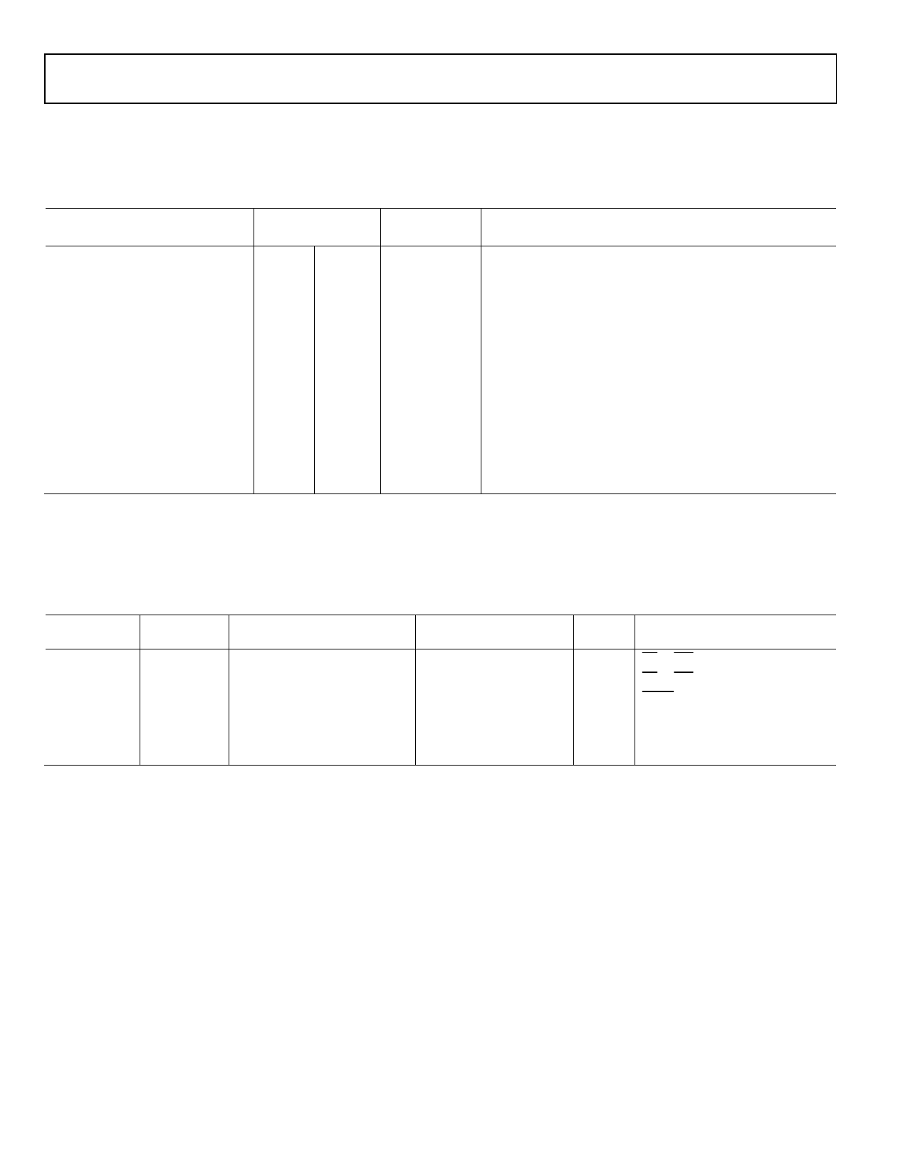
ORDERING GUIDE
Model
Temperature
Range
AD7538JN
AD7538KN
AD7538JR
AD7538KR
AD7538AQ
AD7538BQ
AD7538SQ
AD7538TQ
0°C to +70°C
0°C to +70°C
0°C to +70°C
0°C to +70°C
–25°C to +85°C
–25°C to +85°C
–55°C to +125°C
–55°C to +125°C
*N = Plastic DIP; Q = Cerdip; R = SOIC.
Relative
Accuracy
± 2 LSB
± 1 LSB
± 2 LSB
± 1 LSB
± 2 LSB
± 1 LSB
± 2 LSB
± 1 LSB
Full-Scale Package
Error
Option*
± 8 LSB
± 4 LSB
± 8 LSB
± 4 LSB
± 8 LSB
± 4 LSB
± 8 LSB
± 4 LSB
N-24
N-24
R-24
R-24
Q-24
Q-24
Q-24
Q-24
Pin
11
12
13
14
15
6–19
20
21
22
Mnemonic
VREF
RFB
IOUT
AGND
DGND
DB13–DB0
LDAC
CS
WR
23
VDD
24
VSS
PIN FUNCTION DESCRIPTION
Description
Voltage Reference.
Feedback Resistor. Used to close the loop around an external op amp.
Current Output Terminal.
Analog Ground
Digital Ground
Data Inputs. Bit 13 (MSB) to Bit 0 (LSB).
Chip Select Input. Active LOW.
Asynchronous Load DAC Input. Active LOW.
Write Input. Active LOW.
CS
LDAC
WR
OPERATION
0
1
1
0
0
0
1
1
X
1
0
Load Input Register.
X
Load DAC Register from Input Register.
0
Input and DAC Registers are Transparent.
X
No Operation.
1
No Operation.
NOTE: X Don’t Care.
+12 V to +15 V supply input.
Bias pin for High Temperature Low Leakage configuration. To implement low leakage
system, the pin should be at a negative voltage. See Figures 4 and 5 for recommended circuitry.
–4–
REV. A
Share Link: 